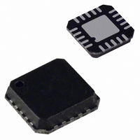
AD8328ACP-REEL Analog Devices Inc, AD8328ACP-REEL Datasheet - Page 13

AD8328ACP-REEL
Manufacturer Part Number
AD8328ACP-REEL
Description
IC LINE DRIVE CBLE 5V 20LFCSP TR
Manufacturer
Analog Devices Inc
Type
Line Driver, Transmitterr
Datasheet
1.AD8328ARQZ.pdf
(20 pages)
Specifications of AD8328ACP-REEL
Rohs Status
RoHS non-compliant
Applications
Modems, Set-Top Boxes
Mounting Type
Surface Mount
Package / Case
20-LFCSP
DIFFERENTIAL SIGNAL SOURCE
Typical applications for the AD8328 use a differential input
signal from a modulator or a DAC. See Table 7 for common
values of R4, or calculate other input configurations using
Equation 2. This circuit configuration will give optimal
distortion results due to the symmetric input signals. Note
that this configuration was used to characterize the AD8328.
DIFFERENTIAL SIGNAL FROM SINGLE-ENDED
SOURCE
The default configuration of the evaluation board implements
a differential signal drive from a single-ended signal source.
This configuration uses a 1:1 balun transformer to approximate
a differential signal. Because of the nonideal nature of real
transformers, the differential signal is not purely equal and
opposite in amplitude. Although this circuit slightly sacrifices
even-order harmonic distortion due to asymmetry, it does
provide a convenient way to evaluate the AD8328 with a single-
ended source.
The AD8328 evaluation board is populated with a TOKO
617DB-A0070 1:1 for this purpose (T1). Table 7 provides
typical R4 values for common input configurations. Other input
impedances can be calculated using Equation 3. See Figure 26
for a schematic of the evaluation board. To use the transformer
for converting a single-ended source into a differential signal,
the input signal must be applied to V
SINGLE-ENDED SOURCE
Although the AD8328 was designed to have optimal DOCSIS
performance when used with a differential input signal, the
AD8328 can also be used as a single-ended receiver, or an IF
digitally controlled amplifier. However, as with the single-
ended-to-differential configuration previously noted, even-
order harmonic distortion is slightly degraded.
When operating the AD8328 in a single-ended input mode,
V
On the AD8328 evaluation boards, this termination method
IN+
and V
R4
R4
Z
IN
=
=
Z
1.6
1.6
Z
IN
Z
IN–
IN
IN
should be terminated as shown in Figure 23.
kΩ
kΩ
V
×
×
IN+
Figure 22. Single-to-Differential Circuit
1.6
1.6
V
V
−
IN+
IN–
−
Z
Z
kΩ
kΩ
Figure 21. Differential Circuit
IN
IN
R4
R4
IN+
.
AD8328
AD8328
Rev. A | Page 13 of 20
(2)
(3)
requires the removal of R2 and R3 to be shorted with R4 open,
as well as the addition of 82.5 Ω at R1 and 39.2 Ω at R17 for
75 Ω termination. Table 7 shows the correct values for R11
and R12 for some common input configurations. Other input
impedance configurations can be accommodated using
Equation 4 and Equation 5.
Table 7. Common Matching Resistors
Z
50
75
100
150
Z
50
75
OVERSHOOT ON PC PRINTER PORTS
The data lines on some PC parallel printer ports have excessive
overshoot that can cause communication problems when
presented to the CLK pin of the AD8328. The evaluation
board was designed to accommodate a series resistor and
shunt capacitor (R2 and C5 in Figure 26) to filter the CLK
signal if required.
INSTALLING VISUAL BASIC CONTROL SOFTWARE
Install the CabDrive_28 software by running the setup.exe file
on Disk One of the AD8328 evaluation software. Follow the on-
screen directions and insert Disk Two when prompted. Choose
the installation directory and then select the icon in the upper
left to complete the installation.
IN
IN
(Ω)
(Ω)
R
R
1
17
=
=
Z
800
Z
IN
R
Z
R2/R3
Open
Open
Open
Open
R2 (Ω)/R3 (Ω)
0/0
0/0
IN
1
IN
−
+
×
Single-Ended Input Termination
×
V
Z
Differential Input Termination
800
Z
IN+
R
IN
IN
1
Figure 23. Single-Ended Circuit
R1
R17
R4 (Ω)
51.1
78.7
107.0
165.0
R4 (Ω)
Open
Open
AD8328
R1/R17
Open/Open
Open/Open
Open/Open
Open/Open
R1 (Ω)/R17 (Ω)
53.6/25.5
82.5/39.2
AD8328
(4)
(5)


