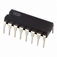
74HCT367N,652 NXP Semiconductors, 74HCT367N,652 Datasheet - Page 2

74HCT367N,652
Manufacturer Part Number
74HCT367N,652
Description
IC BUFF DVR TRI-ST HEX 16PDIP
Manufacturer
NXP Semiconductors
Series
74HCTr
Datasheet
1.74HCT367N652.pdf
(7 pages)
Specifications of 74HCT367N,652
Logic Type
Buffer/Line Driver, Non-Inverting
Package / Case
16-DIP (0.300", 7.62mm)
Number Of Elements
2
Number Of Bits Per Element
2, 4 (Hex)
Current - Output High, Low
6mA, 6mA
Voltage - Supply
4.5 V ~ 5.5 V
Operating Temperature
-40°C ~ 125°C
Mounting Type
Through Hole
Logic Family
74HCT
Number Of Channels Per Chip
6
Polarity
Non-Inverting
Supply Voltage (max)
5.5 V
Supply Voltage (min)
4.5 V
Maximum Operating Temperature
125 C
Mounting Style
SMD/SMT
High Level Output Current
- 6 mA
Input Bias Current (max)
8 uA
Low Level Output Current
6 mA
Maximum Power Dissipation
750 mW
Minimum Operating Temperature
- 40 C
Number Of Lines (input / Output)
8 / 6
Output Type
3-State
Propagation Delay Time
11 ns
Logical Function
Buffer/Line Driver
Number Of Elements
2
Number Of Channels
6
Number Of Inputs
6
Number Of Outputs
6
Operating Supply Voltage (typ)
5V
Package Type
PDIP
Operating Supply Voltage (max)
5.5V
Operating Supply Voltage (min)
4.5V
Quiescent Current
8uA
Technology
CMOS
Pin Count
16
Mounting
Through Hole
Operating Temp Range
-40C to 125C
Operating Temperature Classification
Automotive
Lead Free Status / RoHS Status
Lead free / RoHS Compliant
Lead Free Status / RoHS Status
Lead free / RoHS Compliant, Lead free / RoHS Compliant
Other names
568-1539-5
74HCT367N
933670230652
74HCT367N
933670230652
Philips Semiconductors
FEATURES
GENERAL DESCRIPTION
The 74HC/HCT367 are high-speed Si-gate CMOS devices
and are pin compatible with low power Schottky TTL
(LSTTL). They are specified in compliance with JEDEC
standard no. 7.
QUICK REFERENCE DATA
GND = 0 V; T
Notes
1. C
2. For HC the condition is V
ORDERING INFORMATION
See
December 1990
t
C
C
PHL
Non-inverting outputs
Output capability: bus driver
I
Hex buffer/line driver; 3-state
I
PD
CC
SYMBOL
f
f
C
V
For HCT the condition is V
i
o
“74HC/HCT/HCU/HCMOS Logic Package Information”
/ t
CC
PD
L
category: MSI
= output frequency in MHz
= input frequency in MHz
(C
PLH
= output load capacitance in pF
P
is used to determine the dynamic power dissipation (P
= supply voltage in V
L
D
= C
V
amb
CC
PD
2
= 25 C; t
propagation delay nA to nY
input capacitance
power dissipation capacitance per buffer
V
f
o
CC
) = sum of outputs
2
f
r
i
= t
I
I
f
= GND to V
= GND to V
= 6 ns
(C
PARAMETER
L
V
CC
2
CC
CC
f
o
) where:
1.5 V
2
.
The 74HC/HCT367 are hex non-inverting buffer/line
drivers with 3-state outputs. The 3-state outputs (nY) are
controlled by the output enable inputs (1OE, 2OE).
A HIGH on nOE causes the outputs to assume a high
impedance OFF-state.
The “367” is identical to the “368” but has non-inverting
outputs.
D
C
notes 1 and 2
in W):
L
= 15 pF; V
CONDITIONS
CC
= 5 V
8
3.5
30
HC
TYPICAL
74HC/HCT367
Product specification
11
3.5
32
HCT
ns
pF
pF
UNIT


