MC74HCT541ADWG ON Semiconductor, MC74HCT541ADWG Datasheet
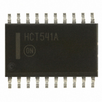
IC BUFF/DVR TRI-ST 8BIT 20SOIC

MC74HCT541ADWG

Manufacturer Part Number
MC74HCT541ADWG
Description
IC BUFF/DVR TRI-ST 8BIT 20SOIC
Manufacturer
ON Semiconductor
Series
74HCTr
Datasheets

Specifications of MC74HCT541ADWG

Logic Type
Buffer/Line Driver, Non-Inverting
Number Of Elements
1
Number Of Bits Per Element
8
Current - Output High, Low
6mA, 6mA
Voltage - Supply
4.5 V ~ 5.5 V
Operating Temperature
-55°C ~ 125°C
Mounting Type
Surface Mount
Package / Case
20-SOIC (7.5mm Width)
Logic Family
74HCT
Number Of Channels Per Chip
Octal
Polarity
Non-Inverting
Supply Voltage (max)
5.5 V
Supply Voltage (min)
4.5 V
Maximum Operating Temperature
125 C
Mounting Style
SMD/SMT
High Level Output Current
- 6 mA
Input Bias Current (max)
4 uA
Low Level Output Current
6 mA
Maximum Power Dissipation
500 mW
Minimum Operating Temperature
- 55 C
Number Of Lines (input / Output)
3
Output Type
3-State
Propagation Delay Time
23 ns @ 5 V
Circuit Type
Silicon Gate
Current, Supply
160 μA
Function Type
8-Channels
Logic Function
Buffer/Driver/Receiver
Number Of Circuits
Octal
Package Type
SOIC-20
Special Features
Non-Inverting, Tri-State
Temperature, Operating, Range
-55 to +125 °C
Voltage, Supply
4.5 to 5.5 V
Lead Free Status / RoHS Status
Lead free / RoHS Compliant
Other names
MC74HCT541ADWG
MC74HCT541ADWGOS

Available stocks

Company
Part Number
Manufacturer
Quantity
Price
Part Number:
MC74HCT541ADWG
Manufacturer:
Freescale
Quantity:
540
MC74HCT541A
Octal 3−State Non−Inverting
Buffer/Line Driver/
Line Receiver With
LSTTL−Compatible Inputs
High−Performance Silicon−Gate CMOS
device may be used as a level converter for interfacing TTL or NMOS
outputs to high speed CMOS inputs.
receiver designed to be used with 3−state memory address drivers,
clock drivers, and other bus−oriented systems. This device features
inputs and outputs on opposite sides of the package and two ANDed
active−low output enables.
Features
*For additional information on our Pb−Free strategy and soldering details, please
© Semiconductor Components Industries, LLC, 2006
June, 2006 − Rev. 5
download the ON Semiconductor Soldering and Mounting Techniques
Reference Manual, SOLDERRM/D.
The MC74HCT541A is identical in pinout to the LS541. This
The HCT541A is an octal non−inverting buffer/line driver/line
Output Drive Capability: 15 LSTTL Loads
TTL/NMOS−Compatible Input Levels
Outputs Directly Interface to CMOS, NMOS and TTL
Operating Voltage Range: 4.5 to 5.5 V
Low Input Current: 1mA
In Compliance With the JEDEC Standard No. 7A Requirements
Chip Complexity: 134 FETs or 33.5 Equivalent Gates
Pb−Free Packages are Available*
Enables
Output
Inputs
Data
OE1
OE2
A1
A2
A3
A4
A5
A6
A7
A8
2
3
4
5
6
7
8
9
1
19
LOGIC DIAGRAM
PIN 20 = V
PIN 10 = GND
18
17
16
15
14
13
12
11
CC
Y1
Y2
Y3
Y4
Y5
Y6
Y7
Y8
Non−Inverting
Outputs
1
See detailed ordering and shipping information in the package
dimensions section on page 5 of this data sheet.
SOIC−20WB
DW SUFFIX
CASE 751D
CASE 948E
SOEIAJ−20
DT SUFFIX
TSSOP−20
CASE 738
1
CASE 967
N SUFFIX
F SUFFIX
PDIP−20
ORDERING INFORMATION
1
1
(Note: Microdot may be in either location)
1
http://onsemi.com
A
WL, L
YY, Y
WW, W = Work Week
G or G
20
1
20
20
1
MARKING DIAGRAMS
1
= Assembly Location
= Wafer Lot
= Year
= Pb−Free Package
Publication Order Number:
20
1
MC74HCT541AN
AWLYYWWG
AWLYYWWG
74HCT541A
AWLYWWG
HCT541A
ALYWG
MC74HCT541A/D
541A
HCT
G

Related parts for MC74HCT541ADWG

MC74HCT541ADWG Summary of contents

Page 1

... Output OE1 OE2 Enables 19 *For additional information on our Pb−Free strategy and soldering details, please download the ON Semiconductor Soldering and Mounting Techniques Reference Manual, SOLDERRM/D. © Semiconductor Components Industries, LLC, 2006 June, 2006 − Rev. 5 SOIC−20WB DW SUFFIX CASE 751D CASE 948E ...

Page 2

... Plastic DIP: – 10 mW/_C from 65_ to 125_C SOIC Package: – 7 mW/_C from 65_ to 125_C For high frequency or heavy load considerations, see Chapter 2 of the ON Semiconductor High−Speed CMOS Data Book (DL129/D). RECOMMENDED OPERATING CONDITIONS Î Î Î Î ...

Page 3

... Maximum Input Leakage Current in I Maximum 3−State Leakage Current OZ I Maximum Quiescent Supply Current CC (per Package) DI Additional Quiescent Supply Current CC 1. Information on typical parametric values can be found in Chapter 2 of the ON Semiconductor High−Speed CMOS Data Book (DL129/D). + ΣDI 2. Total Supply Current = CHARACTERISTICS (V = 5.0V Symbol t ...

Page 4

INPUT A t PLH OUTPUT Y OE1 or OE2 OUTPUT Y OUTPUT Y TEST POINT OUTPUT DEVICE UNDER C * TEST L *Includes all probe and jig capacitance Figure 3. MC74HCT541A SWITCHING WAVEFORMS t f 90% 1.3V 10% ...

Page 5

... One of Eight INPUT A OE1 OE2 ORDERING INFORMATION Device MC74HCT541AN MC74HCT541ANG MC74HCT541ADW MC74HCT541ADWG MC74HCT541ADWR2 MC74HCT541ADWR2G MC74HCT541ADTR2 MC74HCT541ADTR2G MC74HCT541AFG MC74HCT541AFEL MC74HCT541AFELG †For information on tape and reel specifications, including part orientation and tape sizes, please refer to our Tape and Reel Packaging Specifications Brochure, BRD8011/D. ...

Page 6

SEATING PLANE 0.25 (0.010 20X T 0. 18X A1 MC74HCT541A PACKAGE DIMENSIONS PDIP−20 N SUFFIX CASE ...

Page 7

K 20X REF 0.10 (0.004) 0.15 (0.006 L PIN 1 IDENT 1 0.15 (0.006 −V− 0.100 (0.004) −T− SEATING PLANE MC74HCT541A PACKAGE DIMENSIONS TSSOP−20 DT SUFFIX CASE ...

Page 8

... Opportunity/Affirmative Action Employer. This literature is subject to all applicable copyright laws and is not for resale in any manner. PUBLICATION ORDERING INFORMATION LITERATURE FULFILLMENT: Literature Distribution Center for ON Semiconductor P.O. Box 5163, Denver, Colorado 80217 USA Phone: 303−675−2175 or 800−344−3860 Toll Free USA/Canada Fax: 303− ...

Related keywords