MC74HCT541ADWG ON Semiconductor, MC74HCT541ADWG Datasheet - Page 5
MC74HCT541ADWG
Manufacturer Part Number
MC74HCT541ADWG
Description
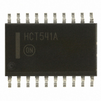
IC BUFF/DVR TRI-ST 8BIT 20SOIC
Manufacturer
ON Semiconductor
Series
74HCTr
Specifications of MC74HCT541ADWG
Logic Type
Buffer/Line Driver, Non-Inverting
Number Of Elements
1
Number Of Bits Per Element
8
Current - Output High, Low
6mA, 6mA
Voltage - Supply
4.5 V ~ 5.5 V
Operating Temperature
-55°C ~ 125°C
Mounting Type
Surface Mount
Package / Case
20-SOIC (7.5mm Width)
Logic Family
74HCT
Number Of Channels Per Chip
Octal
Polarity
Non-Inverting
Supply Voltage (max)
5.5 V
Supply Voltage (min)
4.5 V
Maximum Operating Temperature
125 C
Mounting Style
SMD/SMT
High Level Output Current
- 6 mA
Input Bias Current (max)
4 uA
Low Level Output Current
6 mA
Maximum Power Dissipation
500 mW
Minimum Operating Temperature
- 55 C
Number Of Lines (input / Output)
3
Output Type
3-State
Propagation Delay Time
23 ns @ 5 V
Circuit Type
Silicon Gate
Current, Supply
160 μA
Function Type
8-Channels
Logic Function
Buffer/Driver/Receiver
Number Of Circuits
Octal
Package Type
SOIC-20
Special Features
Non-Inverting, Tri-State
Temperature, Operating, Range
-55 to +125 °C
Voltage, Supply
4.5 to 5.5 V
Lead Free Status / RoHS Status
Lead free / RoHS Compliant
Other names
MC74HCT541ADWG
MC74HCT541ADWGOS
MC74HCT541ADWGOS
Available stocks
Company
Part Number
Manufacturer
Quantity
Price
Company:

Part Number:
MC74HCT541ADWG
Manufacturer:
Freescale
Quantity:
540


INPUTS
9) — Data input pins. Data on these pins appear in
non−inverted form on the corresponding Y outputs, when
the outputs are enabled.
CONTROLS
When a low voltage is applied to both of these pins, the
†For information on tape and reel specifications, including part orientation and tape sizes, please refer to our Tape and Reel Packaging
*These packages are inherently Pb−Free.
ORDERING INFORMATION
Specifications Brochure, BRD8011/D.
MC74HCT541AN
MC74HCT541ANG
MC74HCT541ADW
MC74HCT541ADWG
MC74HCT541ADWR2
MC74HCT541ADWR2G
MC74HCT541ADTR2
MC74HCT541ADTR2G
MC74HCT541AFG
MC74HCT541AFEL
MC74HCT541AFELG
A1, A2, A3, A4, A5, A6, A7, A8 (PINS 2, 3, 4, 5, 6, 7, 8,
OE1, OE2 (PINS 1, 19) — Output enables (active−low).
Device
INPUT A
OE1
OE2
One of Eight
Buffers
To 7 Other
Buffers
PIN DESCRIPTIONS
http://onsemi.com
MC74HCT541A
LOGIC DETAIL
TSSOP−20*
TSSOP−20*
SOEIAJ−20
SOEIAJ−20
SOEIAJ−20
(Pb−Free)
(Pb−Free)
(Pb−Free)
(Pb−Free)
(Pb−Free)
Package
SOIC−20
SOIC−20
SOIC−20
SOIC−20
PDIP−20
PDIP−20
5
outputs are enabled and the device functions as a
non−inverting buffer. When a high voltage is applied to
either input, the outputs assume the high impedance state.
OUTPUTS
13, 12, 11) — Device outputs. Depending upon the state of
the output enable pins, these outputs are either
non−inverting outputs or high−impedance outputs.
Y1, Y2, Y3, Y4, Y5, Y6, Y7, Y8 (PINS 18, 17, 16, 15, 14,
V
CC
OUTPUT Y
1000 / Tape & Reel
2500 / Tape & Reel
2000 / Tape & Reel
18 Units / Rail
38 Units / Rail
40 Units / Rail
Shipping
†
Related parts for MC74HCT541ADWG
Image
Part Number
Description
Manufacturer
Datasheet
Request
R

Part Number:
Description:
ON Semiconductor [VOLTAGE REGULATOR]
Manufacturer:
ON Semiconductor
Datasheet:
Part Number:
Description:
357-036-542-201 CARDEDGE 36POS DL .156 BLK LOPRO
Manufacturer:
ON Semiconductor
Datasheet:
Part Number:
Description:
357-036-542-201 CARDEDGE 36POS DL .156 BLK LOPRO
Manufacturer:
ON Semiconductor
Datasheet:
Part Number:
Description:
357-036-542-201 CARDEDGE 36POS DL .156 BLK LOPRO
Manufacturer:
ON Semiconductor
Datasheet:
Part Number:
Description:
357-036-542-201 CARDEDGE 36POS DL .156 BLK LOPRO
Manufacturer:
ON Semiconductor
Datasheet:
Part Number:
Description:
357-036-542-201 CARDEDGE 36POS DL .156 BLK LOPRO
Manufacturer:
ON Semiconductor
Datasheet:
Part Number:
Description:
357-036-542-201 CARDEDGE 36POS DL .156 BLK LOPRO
Manufacturer:
ON Semiconductor
Datasheet:
Part Number:
Description:
357-036-542-201 CARDEDGE 36POS DL .156 BLK LOPRO
Manufacturer:
ON Semiconductor
Datasheet:
Part Number:
Description:
357-036-542-201 CARDEDGE 36POS DL .156 BLK LOPRO
Manufacturer:
ON Semiconductor
Datasheet:
Part Number:
Description:
357-036-542-201 CARDEDGE 36POS DL .156 BLK LOPRO
Manufacturer:
ON Semiconductor
Datasheet:
Part Number:
Description:
357-036-542-201 CARDEDGE 36POS DL .156 BLK LOPRO
Manufacturer:
ON Semiconductor
Datasheet:
Part Number:
Description:
Manufacturer:
ON Semiconductor
Datasheet:
Part Number:
Description:
Manufacturer:
ON Semiconductor
Datasheet:
Part Number:
Description:
Manufacturer:
ON Semiconductor
Datasheet: