MC74VHC1G50DFT2G ON Semiconductor, MC74VHC1G50DFT2G Datasheet
MC74VHC1G50DFT2G
Manufacturer Part Number
MC74VHC1G50DFT2G
Description
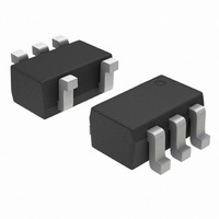
IC BUFFER CMOS NON-INV SOT353
Manufacturer
ON Semiconductor
Series
74VHCr
Datasheet
1.MC74VHC1G50DFT2G.pdf
(8 pages)
Specifications of MC74VHC1G50DFT2G
Logic Type
Buffer/Line Driver, Non-Inverting
Number Of Elements
1
Number Of Bits Per Element
1
Current - Output High, Low
8mA, 8mA
Voltage - Supply
2 V ~ 5.5 V
Operating Temperature
-55°C ~ 125°C
Mounting Type
Surface Mount
Package / Case
SC-70-5, SC-88A, SOT-323-5, SOT-353, 5-TSSOP
Logic Family
VHC
Number Of Channels Per Chip
1
Polarity
Non-Inverting
Supply Voltage (max)
5.5 V
Supply Voltage (min)
2 V
Maximum Operating Temperature
+ 125 C
Mounting Style
SMD/SMT
High Level Output Current
- 8 mA
Low Level Output Current
8 mA
Maximum Power Dissipation
200 mW
Minimum Operating Temperature
- 55 C
Number Of Lines (input / Output)
1 / 1
Propagation Delay Time
10.6 ns at 3.3 V, 7.5 ns at 5 V
Lead Free Status / RoHS Status
Lead free / RoHS Compliant
Other names
MC74VHC1G50DFT2GOS
MC74VHC1G50DFT2GOS
MC74VHC1G50DFT2GOSTR
MC74VHC1G50DFT2GOS
MC74VHC1G50DFT2GOSTR
Available stocks
Company
Part Number
Manufacturer
Quantity
Price

Part Number:
MC74VHC1G50DFT2G
Manufacturer:
ON/安森美
Quantity:
20 000


MC74VHC1G50
Buffer
fabricated with silicon gate CMOS technology. It achieves high speed
operation similar to equivalent Bipolar Schottky TTL while maintaining
CMOS low power dissipation.
output which provides high noise immunity and stable output.
voltages up to 7.0 V are applied, regardless of the supply voltage. This
allows the MC74VHC1G50 to be used to interface 5.0 V circuits to 3.0 V
circuits.
•
•
•
•
•
•
•
© Semiconductor Components Industries, LLC, 2006
March, 2006 - - Rev. 12
The MC74VHC1G50 is an advanced high speed CMOS buffer
The internal circuit is composed of three stages, including a buffered
The MC74VHC1G50 input structure provides protection when
These devices are available in Pb- -free package(s). Specifications herein
apply to both standard and Pb- -free devices. Please see our website at
www.onsemi.com for specific Pb- -free orderable part numbers, or
contact your local ON Semiconductor sales office or representative.
High Speed: t
Low Power Dissipation: I
Power Down Protection Provided on Inputs
Balanced Propagation Delays
Pin and Function Compatible with Other Standard Logic Families
Chip Complexity: FET = 104; Equivalent Gate = 26
GND
IN A
PD
NC
IN A
= 3.5 ns (Typ) at V
Figure 1. Pinout (Top View)
1
2
3
Figure 2. Logic Symbol
CC
= 1 mA (Max) at T
1
CC
= 5 V
5
4
OUT Y
A
V
OUT Y
CC
= 25°C
1
See detailed ordering and shipping information in the package
dimensions section on page 4 of this data sheet.
1
2
4
3
5
SC- -88A / SOT- -353/SC- -70
A Input
ORDERING INFORMATION
TSOP- -5/SOT- -23/SC- -59
H
L
http://onsemi.com
PIN ASSIGNMENT
FUNCTION TABLE
CASE 419A
DF SUFFIX
DT SUFFIX
CASE 483
Publication Order Number:
OUT Y
GND
IN A
V
NC
CC
MC74VHC1G50/D
Y Output
DIAGRAMS
Pin 1
d = Date Code
Pin 1
d = Date Code
MARKING
H
L
VR
VR
d
d
Related parts for MC74VHC1G50DFT2G
Image
Part Number
Description
Manufacturer
Datasheet
Request
R

Part Number:
Description:
ON Semiconductor [VOLTAGE REGULATOR]
Manufacturer:
ON Semiconductor
Datasheet:
Part Number:
Description:
357-036-542-201 CARDEDGE 36POS DL .156 BLK LOPRO
Manufacturer:
ON Semiconductor
Datasheet:
Part Number:
Description:
357-036-542-201 CARDEDGE 36POS DL .156 BLK LOPRO
Manufacturer:
ON Semiconductor
Datasheet:
Part Number:
Description:
357-036-542-201 CARDEDGE 36POS DL .156 BLK LOPRO
Manufacturer:
ON Semiconductor
Datasheet:
Part Number:
Description:
357-036-542-201 CARDEDGE 36POS DL .156 BLK LOPRO
Manufacturer:
ON Semiconductor
Datasheet:
Part Number:
Description:
357-036-542-201 CARDEDGE 36POS DL .156 BLK LOPRO
Manufacturer:
ON Semiconductor
Datasheet:
Part Number:
Description:
357-036-542-201 CARDEDGE 36POS DL .156 BLK LOPRO
Manufacturer:
ON Semiconductor
Datasheet:
Part Number:
Description:
357-036-542-201 CARDEDGE 36POS DL .156 BLK LOPRO
Manufacturer:
ON Semiconductor
Datasheet:
Part Number:
Description:
357-036-542-201 CARDEDGE 36POS DL .156 BLK LOPRO
Manufacturer:
ON Semiconductor
Datasheet:
Part Number:
Description:
357-036-542-201 CARDEDGE 36POS DL .156 BLK LOPRO
Manufacturer:
ON Semiconductor
Datasheet:
Part Number:
Description:
357-036-542-201 CARDEDGE 36POS DL .156 BLK LOPRO
Manufacturer:
ON Semiconductor
Datasheet:
Part Number:
Description:
Manufacturer:
ON Semiconductor
Datasheet:
Part Number:
Description:
Manufacturer:
ON Semiconductor
Datasheet:
Part Number:
Description:
Manufacturer:
ON Semiconductor
Datasheet: