74ABT244CMTC Fairchild Semiconductor, 74ABT244CMTC Datasheet
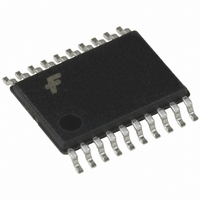
IC BUFF/DVR TRI-ST DUAL 20TSSOP

74ABT244CMTC

Manufacturer Part Number
74ABT244CMTC
Description
IC BUFF/DVR TRI-ST DUAL 20TSSOP
Manufacturer
Fairchild Semiconductor
Series
74ABTr
Datasheets

Specifications of 74ABT244CMTC

Logic Type
Buffer/Line Driver, Non-Inverting
Number Of Elements
2
Number Of Bits Per Element
4
Current - Output High, Low
32mA, 64mA
Voltage - Supply
4.5 V ~ 5.5 V
Operating Temperature
-40°C ~ 85°C
Mounting Type
Surface Mount
Package / Case
20-TSSOP
Logic Family
ABT
Number Of Channels Per Chip
8
Polarity
Non-Inverting
Supply Voltage (max)
5.5 V
Supply Voltage (min)
4.5 V
Maximum Operating Temperature
+ 85 C
Mounting Style
SMD/SMT
High Level Output Current
- 32 mA
Low Level Output Current
64 mA
Minimum Operating Temperature
- 40 C
Number Of Lines (input / Output)
8 / 3
Output Type
3-State
Propagation Delay Time
3.6 ns at 5 V
Lead Free Status / RoHS Status
Lead free / RoHS Compliant

Available stocks

Company
Part Number
Manufacturer
Quantity
Price
Part Number:
74ABT244CMTCX
Manufacturer:
FAIRCHILD/仙童
Quantity:
20 000
© 1999 Fairchild Semiconductor Corporation
74ABT244CSC
74ABT244CSJ
74ABT244CMSA
74ABT244CMTC
74ABT244CPC
74ABT244
Octal Buffer/Line Driver with 3-STATE Outputs
General Description
The ABT244 is an octal buffer and line driver with 3-STATE
outputs designed to be employed as a memory and
address driver, clock driver, or bus-oriented transmitter/
receiver.
Ordering Code:
Device also available in Tape and Reel. Specify by appending suffix letter “X” to the ordering code.
Connection Diagram
Order Number
Package Number
MSA20
MTC20
M20B
M20D
N20A
20-Lead Small Outline Integrated Circuit (SOIC), JEDEC MS-013, 0.300” Wide Body
20-Lead Small Outline Package (SOP), EIAJ TYPE II, 5.3mm Wide
20-Lead Shrink Small Outline Package (SSOP), EIAJ TYPE II, 5.3mm Wide
20-Lead Thin Shrink Small Outline Package (TSSOP), JEDEC MO-153, 4.4mm Wide
20-Lead Plastic Dual-In-Line Package (PDIP), JEDEC MS-001, 0.300” Wide
DS010992
Features
Pin Descriptions
Truth Table
H
L
X
Z
Non-inverting buffers
Output sink capability of 64 mA, source capability of
32 mA
Guaranteed output skew
Guaranteed multiple output switching specifications
Output switching specified for both 50 pF and 250 pF
loads
Guaranteed simultaneous switching, noise level and
dynamic threshold performance
Guaranteed latchup protection
High impedance glitch free bus loading during entire
power up and power down cycle
Nondestructive hot insertion capability
Disable time less than enable time to avoid bus conten-
tion
LOW Voltage Level
Immaterial
High Impedance
HIGH Voltage Level
OE
I
O
Package Description
0
OE
Pin Names
–I
0
H
–O
L
L
1
7
, OE
1
7
2
I
0–3
X
H
L
Output Enable Input
Inputs
Outputs
O
(Active LOW)
H
0–3
Z
L
May 1992
Revised November 1999
Description
OE
H
L
L
2
www.fairchildsemi.com
I
4–7
X
H
L
O
Z
H
4–7
L

Related parts for 74ABT244CMTC

74ABT244CMTC Summary of contents

Page 1

... M20D 20-Lead Small Outline Package (SOP), EIAJ TYPE II, 5.3mm Wide 74ABT244CMSA MSA20 20-Lead Shrink Small Outline Package (SSOP), EIAJ TYPE II, 5.3mm Wide 74ABT244CMTC MTC20 20-Lead Thin Shrink Small Outline Package (TSSOP), JEDEC MO-153, 4.4mm Wide 74ABT244CPC N20A 20-Lead Plastic Dual-In-Line Package (PDIP), JEDEC MS-001, 0.300” Wide Device also available in Tape and Reel. Specify by appending suffix letter “ ...

Page 2

Absolute Maximum Ratings Storage Temperature Ambient Temperature under Bias Junction Temperature under Bias V Pin Potential to Ground Pin CC Input Voltage (Note 2) Input Current (Note 5.0 mA Voltage Applied to Any Output in the ...

Page 3

DC Electrical Characteristics (SOIC package) Symbol Parameter V Quiet Output Maximum Dynamic V OLP OL V Quiet Output Minimum Dynamic V OLV OL V Minimum HIGH Level Dynamic Output Voltage OHV V Minimum HIGH Level Dynamic Input Voltage IHD V ...

Page 4

Skew Symbol Parameter t Pin to Pin Skew OSHL (Note 12) HL Transitions t Pin to Pin Skew OSLH (Note 12) LH Transitions t Duty Cycle PS (Note 16) LH–HL Skew t Pin to Pin Skew OST (Note 12) LH/HL ...

Page 5

AC Loading *Includes jig and probe capacitance FIGURE 1. Standard AC Test Load AC Waveforms FIGURE 2. Test Input Signal Levels Amplitude Rep. Rate 3.0V 1 MHz 500 ns 2.5 ns FIGURE 3. Test Input Signal Requirements ...

Page 6

Physical Dimensions inches (millimeters) unless otherwise noted 20-Lead Small Outline Integrated Circuit (SOIC), JEDEC MS-013, 0.300” Wide Body www.fairchildsemi.com Package Number M20B 6 ...

Page 7

Physical Dimensions inches (millimeters) unless otherwise noted (Continued) 20-Lead Small Outline Package (SOP), EIAJ TYPE II, 5.3mm Wide Package Number M20D 7 www.fairchildsemi.com ...

Page 8

Physical Dimensions inches (millimeters) unless otherwise noted (Continued) 20-Lead Shrink Small Outline Package (SSOP), EIAJ TYPE II, 5.3mm Wide www.fairchildsemi.com Package Number MSA20 8 ...

Page 9

Physical Dimensions inches (millimeters) unless otherwise noted (Continued) 20-Lead Thin Shrink Small Outline Package (TSSOP), JEDEC MO-153, 4.4mm Wide Package Number MTC20 9 www.fairchildsemi.com ...

Page 10

Physical Dimensions inches (millimeters) unless otherwise noted (Continued) 20-Lead Plastic Dual-In-Line Package (PDIP), JEDEC MS-001, 0.300” Wide Fairchild does not assume any responsibility for use of any circuitry described, no circuit patent licenses are implied and Fairchild reserves the right ...

Related keywords