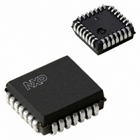
74ABT899A,602 NXP Semiconductors, 74ABT899A,602 Datasheet - Page 2

74ABT899A,602
Manufacturer Part Number
74ABT899A,602
Description
IC 9BIT DUAL LATCH TXRX 28PLCC
Manufacturer
NXP Semiconductors
Series
74ABTr
Datasheet
1.74ABT899A602.pdf
(16 pages)
Specifications of 74ABT899A,602
Logic Type
Parity Generator/Checker
Number Of Circuits
9-Bit
Current - Output High, Low
32mA, 64mA
Voltage - Supply
4.5 V ~ 5.5 V
Operating Temperature
-40°C ~ 85°C
Mounting Type
Surface Mount
Package / Case
28-PLCC
Number Of Elements
1
Number Of Bits Per Element
9
Lead Free Status / RoHS Status
Lead free / RoHS Compliant
Other names
74ABT899A
74ABT899A
935057630602
74ABT899A
935057630602
Available stocks
Company
Part Number
Manufacturer
Quantity
Price
Company:
Part Number:
74ABT899A,602
Manufacturer:
NXP Semiconductors
Quantity:
10 000
FEATURES
QUICK REFERENCE DATA
ORDERING INFORMATION
Philips Semiconductors
28-Pin Plastic PLCC
28-Pin Plastic SOP
28-Pin Plastic SSOP
1998 Jan 16
SYMBOL
Symmetrical (A and B bus functions are identical)
Selectable generate parity or ”feed-through” parity for A-to-B and
B-to-A directions
Independent transparent latches for A-to-B and B-to-A directions
Selectable ODD/EVEN parity
Continuously checks parity of both A bus and B bus latches as
ERRA and ERRB
Ability to simultaneously generate and check parity
Can simultaneously read/latch A and B bus data
Output capability: +64 mA/–32mA
Latch-up protection exceeds 500mA per Jedec JC40.2 Std 17
ESD protection exceeds 2000 V per MIL STD 883 Method 3015
and 200 V per Machine Model
Power up 3-State
Power-up reset
Live insertion/extraction permitted
9-bit dual latch transceiver with 8-bit parity
generator/checker (3-State)
t
t
t
t
I
C
C
CCZ
PLH
PHL
PLH
PHL
I/O
IN
PACKAGES
Propagation delay
An to Bn or Bn to An
Propagation delay
An to ERRA
Input capacitance
Output capacitance
Total supply current
PARAMETER
TEMPERATURE RANGE
–40 C to +85 C
–40 C to +85 C
–40 C to +85 C
OUTSIDE NORTH AMERICA
2
C
C
V
Outputs disabled; V
Outputs disabled; V
DESCRIPTION
The 74ABT899 is a 9-bit to 9-bit parity transceiver with separate
transparent latches for the A bus and B bus. Either bus can
generate or check parity. The parity bit can be fed-through with no
change or the generated parity can be substituted with the SEL
input.
Parity error checking of the A and B bus latches is continuously
provided with ERRA and ERRB, even with both buses in 3-State.
The 74ABT899 features independent latch enables for the A and B
bus latches, a select pin for ODD/EVEN parity, and separate error
signal output pins for checking parity.
FUNCTIONAL DESCRIPTION
The 74ABT899 has three principal modes of operation which are
outlined below. All modes apply to both the A-to-B and B-to-A
directions.
Transparent latch, Generate parity, Check A and B bus parity:
Bus A (B) communicates to Bus B (A), parity is generated and
passed on to the B (A) Bus as BPAR (APAR). If LEA and LEB are
High and the Mode Select (SEL) is Low, the parity generated from
A0-A7 and B0-B7 can be checked and monitored by ERRA and
ERRB. (Fault detection on both input and output buses.)
Transparent latch, Feed-through parity, Check A and B bus
parity:
Bus A (B) communicates to Bus B (A) in a feed-through mode if SEL
is High. Parity is still generated and checked as ERRA and ERRB
and can be used as an interrupt to signal a data/parity bit error to the
CPU.
Latched input, Generate/Feed-through parity, Check A (and B)
bus parity:
Independent latch enables (LEA and LEB) allow other permutations of:
L
L
I
74ABT899 DB
= 0V or V
74ABT899 D
74ABT899 A
= 50pF; V
= 50pF; V
Transparent latch / 1 bus latched / both buses latched
Feed-through parity / generate parity
Check in bus parity / check out bus parity / check in and out bus
parity
T
amb
CC
CC
CC
CONDITIONS
= 25 C; GND = 0V
= 5V
= 5V
O
CC
= 0V or V
=5.5V
NORTH AMERICA
74ABT899 DB
74ABT899 A
74ABT899 D
CC
Product specification
74ABT899
TYPICAL
DWG NUMBER
2.9
6.1
853-1623 18864
50
4
7
SOT261-3
SOT136-1
SOT341-1
UNIT
ns
ns
pF
pF
A


