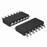
MC74ACT125DG ON Semiconductor, MC74ACT125DG Datasheet - Page 2

MC74ACT125DG
Manufacturer Part Number
MC74ACT125DG
Description
IC BUFF TRI-ST QD N-INV 14SOIC
Manufacturer
ON Semiconductor
Series
74ACTr
Datasheet
1.MC74AC125DTR2G.pdf
(9 pages)
Specifications of MC74ACT125DG
Logic Type
Buffer/Line Driver, Non-Inverting
Number Of Elements
4
Number Of Bits Per Element
1
Current - Output High, Low
24mA, 24mA
Voltage - Supply
4.5 V ~ 5.5 V
Operating Temperature
-40°C ~ 85°C
Mounting Type
Surface Mount
Package / Case
14-SOIC (3.9mm Width), 14-SOL
Logic Family
ACT
Number Of Channels Per Chip
4
Polarity
Non-Inverting
Supply Voltage (max)
5.5 V
Supply Voltage (min)
4.5 V
Maximum Operating Temperature
+ 85 C
Mounting Style
SMD/SMT
High Level Output Current
- 24 mA
Low Level Output Current
24 mA
Minimum Operating Temperature
- 40 C
Number Of Lines (input / Output)
4 / 4
Output Type
3-State
Propagation Delay Time
9 ns at 5 V
Logic Device Type
Buffer, Non Inverting
Supply Voltage Range
4.5V To 5.5V
Logic Case Style
SOIC
No. Of Pins
14
Operating Temperature Range
-40°C To +85°C
Termination Type
SMD
Rohs Compliant
Yes
Filter Terminals
SMD
Family Type
ACT
Lead Free Status / RoHS Status
Lead free / RoHS Compliant
Other names
MC74ACT125DG
MC74ACT125DGOS
MC74ACT125DGOS
Available stocks
Company
Part Number
Manufacturer
Quantity
Price
Company:
Part Number:
MC74ACT125DG
Manufacturer:
ON Semiconductor
Quantity:
5
Stresses exceeding Maximum Ratings may damage the device. Maximum Ratings are stress ratings only. Functional operation above the
Recommended Operating Conditions is not implied. Extended exposure to stresses above the Recommended Operating Conditions may affect
device reliability.
1. V
2. V
MAXIMUM RATINGS
Symbol
RECOMMENDED OPERATING CONDITIONS
Symbol
V
in
V
V
V
T
t
I
I
I
V
I
, V
r
T
T
I
out
CC
OH
OL
stg
, t
CC
out
CC
in
in
in
in
A
J
f
out
from 30% to 70% V
from 0.8 V to 2.0 V; see individual Data Sheets for devices that differ from the typical input rise and fall times.
DC Supply Voltage (Referenced to GND)
DC Input Voltage (Referenced to GND)
DC Output Voltage (Referenced to GND)
DC Input Current, per Pin
DC Output Sink/Source Current, per Pin
DC V
Storage Temperature
Supply Voltage
DC Input Voltage, Output Voltage (Ref. to GND)
Input Rise and Fall Time (Note 1)
′AC Devices except Schmitt Inputs
Junction Temperature (PDIP)
Operating Ambient Temperature Range
Output Current − HIGH
Output Current − LOW
CC
or GND Current per Output Pin
CC
; see individual Data Sheets for devices that differ from the typical input rise and fall times.
Parameter
Parameter
http://onsemi.com
2
V
V
V
CC
CC
CC
′ACT
′AC
@ 3.0 V
@ 4.5 V
@ 5.5 V
Min
−40
2.0
4.5
0
−
−
−
−
−
−
−0.5 to V
−0.5 to V
−0.5 to +7.0
−65 to +150
Value
± 20
± 50
± 50
Typ
150
5.0
5.0
40
25
25
−
−
−
−
CC
CC
+ 0.5
+ 0.5
Max
V
140
−24
6.0
5.5
85
24
CC
−
−
−
ns/V
Unit
Unit
mA
mA
mA
mA
mA
°C
°C
°C
V
V
V
V
V


