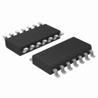
MC74ACT125DG ON Semiconductor, MC74ACT125DG Datasheet - Page 3

MC74ACT125DG
Manufacturer Part Number
MC74ACT125DG
Description
IC BUFF TRI-ST QD N-INV 14SOIC
Manufacturer
ON Semiconductor
Series
74ACTr
Datasheet
1.MC74AC125DTR2G.pdf
(9 pages)
Specifications of MC74ACT125DG
Logic Type
Buffer/Line Driver, Non-Inverting
Number Of Elements
4
Number Of Bits Per Element
1
Current - Output High, Low
24mA, 24mA
Voltage - Supply
4.5 V ~ 5.5 V
Operating Temperature
-40°C ~ 85°C
Mounting Type
Surface Mount
Package / Case
14-SOIC (3.9mm Width), 14-SOL
Logic Family
ACT
Number Of Channels Per Chip
4
Polarity
Non-Inverting
Supply Voltage (max)
5.5 V
Supply Voltage (min)
4.5 V
Maximum Operating Temperature
+ 85 C
Mounting Style
SMD/SMT
High Level Output Current
- 24 mA
Low Level Output Current
24 mA
Minimum Operating Temperature
- 40 C
Number Of Lines (input / Output)
4 / 4
Output Type
3-State
Propagation Delay Time
9 ns at 5 V
Logic Device Type
Buffer, Non Inverting
Supply Voltage Range
4.5V To 5.5V
Logic Case Style
SOIC
No. Of Pins
14
Operating Temperature Range
-40°C To +85°C
Termination Type
SMD
Rohs Compliant
Yes
Filter Terminals
SMD
Family Type
ACT
Lead Free Status / RoHS Status
Lead free / RoHS Compliant
Other names
MC74ACT125DG
MC74ACT125DGOS
MC74ACT125DGOS
Available stocks
Company
Part Number
Manufacturer
Quantity
Price
Company:
Part Number:
MC74ACT125DG
Manufacturer:
ON Semiconductor
Quantity:
5
DC CHARACTERISTICS
Symbol
*All outputs loaded; thresholds on input associated with output under test.
†Maximum test duration 2.0 ms, one input loaded at a time.
NOTE:
AC CHARACTERISTICS
Symbol
*Voltage Range 3.3 V is 3.3 V ±0.3 V.
Voltage Range 5.0 V is 5.0 V ±0.5 V.
I
V
I
t
t
t
t
V
t
t
V
I
OHD
I
V
OLD
PLH
PHL
PZH
PHZ
PZL
PLZ
I
OZ
CC
OH
IN
OL
IH
IL
I
IN
Minimum High Level
Input Voltage
Maximum Low Level
Input Voltage
Minimum High Level
Output Voltage
Minimum Low Level
Output Voltage
Maximum Input
Leakage Current
V
V
V
†Minimum Dynamic
Maximum Quiescent
Supply Current
Propagation Delay
Data to Output
Propagation Delay
Data to Output
Output Enable
Time
Output Enable
Time
Output Disable
Time
Output Disable
Time
Output Current
I
I
O
and I
(OE) = V
= V
= V
CC
CC
CC
, GND
@ 3.0 V are guaranteed to be less than or equal to the respective limit @ 5.5 V.
, GND
IL
, V
IH
Parameter
Parameter
http://onsemi.com
V
(V)
3.0
4.5
5.5
3.0
4.5
5.5
3.0
4.5
5.5
3.0
4.5
5.5
3.0
4.5
5.5
3.0
4.5
5.5
5.5
5.5
5.5
5.5
5.5
CC
3
0.002
0.001
0.001
2.25
2.75
2.25
2.75
2.99
4.46
5.49
Typ
T
1.5
1.5
−
−
−
−
−
−
−
−
−
−
−
A
74AC
= +25°C
3.15
3.85
1.35
1.65
2.56
3.86
4.86
0.36
0.36
0.36
±0.1
±0.5
Guaranteed Limits
2.1
0.9
2.9
4.4
5.4
0.1
0.1
0.1
8.0
−
−
V
(V)
3.3
5.0
3.3
5.0
3.3
5.0
3.3
5.0
3.3
5.0
3.3
5.0
CC
−40°C to
*
74AC
+85°C
T
3.15
3.85
1.35
1.65
2.46
3.76
4.76
0.44
0.44
0.44
±1.0
±5.0
−75
2.1
0.9
2.9
4.4
5.4
0.1
0.1
0.1
75
80
A
=
Min
T
1.0
1.0
1.0
1.0
1.0
1.0
1.0
1.0
1.0
1.0
1.0
1.0
C
A
L
74AC
= +25°C
= 50 pF
Max
10.5
10.5
9.0
7.0
9.0
7.0
7.0
8.0
9.0
9.0
Unit
10
10
mA
mA
mA
mA
mA
V
V
V
V
V
V
Min
T
C
1.0
1.0
1.0
1.0
1.0
1.0
1.0
1.0
1.0
1.0
1.0
1.0
V
or V
V
or V
I
*V
I
I
*V
I
V
V
V
V
V
V
V
OUT
OH
OUT
OL
A
to +85°C
OUT
OUT
I
I
I
O
OLD
OHD
IN
L
IN
IN
(OE) = V
= V
= V
74AC
= −40°C
= 50 pF
= V
= V
CC
CC
= V
= V
= − 50 mA
= 50 mA
= 0.1 V
= 0.1 V
CC
= 1.65 V Max
CC
Conditions
= 3.85 V Min
CC
− 0.1 V
− 0.1 V
CC
Max
10.5
11.5
7.5
7.5
8.0
8.5
9.5
9.5
IL
IL
10
10
11
11
, GND
, GND
, GND
or V
−12 mA
− 24 mA
− 24 mA
or V
12 mA
24 mA
24 mA
or GND
IL
, V
IH
IH
IH
Unit
ns
ns
ns
ns
ns
ns


