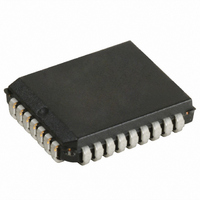
CY7C421-20JXC Cypress Semiconductor Corp, CY7C421-20JXC Datasheet - Page 14

CY7C421-20JXC
Manufacturer Part Number
CY7C421-20JXC
Description
IC ASYNC FIFO MEM 512X9 32-PLCC
Manufacturer
Cypress Semiconductor Corp
Series
CY7Cr
Specifications of CY7C421-20JXC
Access Time
10ns
Memory Size
4.6K (512 x 9)
Package / Case
32-PLCC
Function
Asynchronous
Data Rate
50MHz
Voltage - Supply
3.3V
Operating Temperature
-40°C ~ 85°C
Mounting Type
Surface Mount
Number Of Circuits
2
Data Bus Width
9 bit
Bus Direction
Unidirectional
Timing Type
Asynchronous
Organization
512 K x 9
Supply Voltage (max)
5.5 V
Supply Voltage (min)
4.5 V
Maximum Operating Current
55 mA
Maximum Operating Temperature
+ 70 C
Minimum Operating Temperature
0 C
Mounting Style
SMD/SMT
Configuration
Dual
Density
4.5Kb
Access Time (max)
20ns
Word Size
9b
Sync/async
Asynchronous
Expandable
Yes
Package Type
PLCC
Clock Freq (max)
Not RequiredMHz
Operating Supply Voltage (typ)
5V
Operating Supply Voltage (min)
4.5V
Operating Supply Voltage (max)
5.5V
Supply Current
55mA
Operating Temp Range
0C to 70C
Operating Temperature Classification
Commercial
Mounting
Surface Mount
Pin Count
32
Rohs Compliant
YES
Lead Free Status / RoHS Status
Lead free / RoHS Compliant
Lead Free Status / RoHS Status
Lead free / RoHS Compliant, Lead free / RoHS Compliant
Other names
428-2911-5
CY7C421-20JXC
CY7C421-20JXC
Available stocks
Company
Part Number
Manufacturer
Quantity
Price
Company:
Part Number:
CY7C421-20JXC
Manufacturer:
Cypress Semiconductor Corp
Quantity:
10 000
Part Number:
CY7C421-20JXC
Manufacturer:
CYPRESS/赛普拉斯
Quantity:
20 000
Company:
Part Number:
CY7C421-20JXCT
Manufacturer:
Cypress Semiconductor Corp
Quantity:
10 000
Use of the Empty and Full Flags
To achieve maximum frequency, the flags must be valid at the
beginning of the next cycle. However, because they can be
updated by either edge of the read or write signal, they must be
valid by one-half of a cycle. Cypress FIFOs meet this
requirement; some competitors’ FIFOs do not.
The reason for why the flags should be valid by the next cycle is
complex. The “effective pulse width violation” phenomenon can
occur at the full and empty boundary conditions, if the flags are
not properly used. The empty flag must be used to prevent
reading from an empty FIFO and the full flag must be used to
prevent writing into a full FIFO.
Document #: 38-06001 Rev. *F
FULL
W
D
MR
9
Figure 13. Depth Expansion
9
9
9
FF
FF
FF
CY7C420/1
CY7C424
CY7C428
CY7C432
CY7C420/1
CY7C424
CY7C428
CY7C432
CY7C420/1
CY7C424
CY7C428
CY7C432
XO
XO
XO
XI
XI
XI
For example, consider an empty FIFO that is receiving read
pulses. Because the FIFO is empty, the read pulses are ignored
by the FIFO, and nothing happens. Next, a single word is written
into the FIFO, with a signal that is asynchronous to the read
signal. The (internal) state machine in the FIFO goes from empty
to empty+1. However, it does this asynchronously with respect
to the read signal, so that the effective pulse width of the read
signal cannot be determined, because the state machine does
not look at the read signal until it goes to the empty+1 state.
Similarly, the minimum write pulse width may be violated by
trying to write into a full FIFO, and asynchronously performing a
read. The empty and full flags are used to avoid these effective
pulse width violations, but to do this and operate at the maximum
frequency, the flag must be valid at the beginning of the next
cycle.
*
* FIRST DEVICE
EF
EF
EF
FL
FL
FL
9
CY7C421
Page 14 of 21
Q
EMPTY
R
V
CC
[+] Feedback


