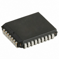
CY7C4291-10JC Cypress Semiconductor Corp, CY7C4291-10JC Datasheet - Page 4

CY7C4291-10JC
Manufacturer Part Number
CY7C4291-10JC
Description
IC DEEP SYNC FIFO 128KX9 32-PLCC
Manufacturer
Cypress Semiconductor Corp
Series
CY7Cr
Datasheet
1.CY7C4291-10JC.pdf
(16 pages)
Specifications of CY7C4291-10JC
Function
Synchronous
Memory Size
1.1M (128K x 9)
Data Rate
100MHz
Access Time
8ns
Voltage - Supply
3.3V
Operating Temperature
-40°C ~ 85°C
Mounting Type
Surface Mount
Package / Case
32-PLCC
Configuration
Dual
Density
1.125Mb
Access Time (max)
8ns
Word Size
9b
Organization
128Kx9
Sync/async
Synchronous
Expandable
Yes
Bus Direction
Uni-Directional
Package Type
PLCC
Clock Freq (max)
100MHz
Operating Supply Voltage (typ)
5V
Operating Supply Voltage (min)
4.5V
Operating Supply Voltage (max)
5.5V
Supply Current
40mA
Operating Temp Range
0C to 70C
Operating Temperature Classification
Commercial
Mounting
Surface Mount
Pin Count
32
Lead Free Status / RoHS Status
Contains lead / RoHS non-compliant
Other names
428-1244
Available stocks
Company
Part Number
Manufacturer
Quantity
Price
Company:
Part Number:
CY7C4291-10JC
Manufacturer:
Cypress Semiconductor Corp
Quantity:
10 000
Document #: 38-06007 Rev. *B
It is not necessary to write to all the offset registers at one time.
A subset of the offset registers can be written; then by bringing
the WEN2/LD input HIGH, the FIFO is returned to normal read
and write operation. The next time WEN2/LD is brought LOW,
a write operation stores data in the next offset register in
sequence.
The contents of the offset registers can be read to the data
outputs when WEN2/LD is LOW and both REN1 and REN2
are LOW. LOW-to-HIGH transitions of RCLK read register
contents to the data outputs. Writes and reads should not be
performed simultaneously on the offset registers.
Programmable Flag (PAE, PAF) Operation
Whether the flag offset registers are programmed as
described in Table 1 or the default values are used, the
programmable almost-empty flag (PAE) and programmable
almost-full flag (PAF) states are determined by their corre-
sponding offset registers and the difference between the read
and write pointers.
Table 1. Writing the Offset Registers
The number formed by the empty offset least significant bit
register and empty offset most significant bit register is
referred to as n and determines the operation of PAE. PAF is
synchronized to the LOW-to-HIGH transition of RCLK by one
flip-flop and is LOW when the FIFO contains n or fewer unread
words. PAE is set HIGH by the LOW-to-HIGH transition of
RCLK when the FIFO contains (n + 1) or greater unread words.
The number formed by the full offset least significant bit
register and full offset most significant bit register is referred to
as m and determines the operation of PAF. PAE is synchro-
nized to the LOW-to-HIGH transition of WCLK by one flip-flop
and is set LOW when the number of unread words in the FIFO
Note:
1.
LD
0
0
1
1
The same selection sequence applies to reading from the registers. REN1 and REN2 are enabled and a read is performed on the LOW-to-HIGH transition of RCLK.
WEN
0
1
0
1
WCLK
[1]
No Operation
Write Into FIFO
No Operation
Empty Offset (LSB)
Empty Offset (MSB)
Full Offset (LSB)
Full Offset (MSB)
Selection
is greater than or equal to CY7C4281 (64K-m) and CY7C4291
(128K-m). PAF is set HIGH by the LOW-to-HIGH transition of
WCLK when the number of available memory locations is
greater than m.
Table 2. Status Flags
Width Expansion Configuration
Word width may be increased simply by connecting the corre-
sponding input controls signals of multiple devices. A
composite flag should be created for each of the end-point
status flags (EF and FF). The partial status flags (PAE and
PAF) can be detected from any one device. Figure 2 demon-
strates a 18-bit word width by using two CY7C42X1s. Any
word width can be attained by adding additional CY7C42X1s.
When the CY7C42X1 is in a Width Expansion Configuration,
the Read Enable (REN2) control input can be grounded (see
Figure 2). In this configuration, the Write Enable 2/Load
(WEN2/LD) pin is set to LOW at Reset so that the pin operates
as a control to load and read the programmable flag offsets.
Flag Operation
The CY7C4281/91 devices provide five flag pins to indicate
the condition of the FIFO contents. Empty, Full, PAE, and PAF
are synchronous.
Full Flag
The Full Flag (FF) will go LOW when the device is full. Write
operations are inhibited whenever FF is LOW regardless of the
state of WEN1 and WEN2/LD. FF is synchronized to WCLK,
i.e., it is exclusively updated by each rising edge of WCLK.
Empty Flag
The Empty Flag (EF) will go LOW when the device is empty.
Read operations are inhibited whenever EF is LOW,
regardless of the state of REN1 and REN2. EF is synchronized
to RCLK, i.e., it is exclusively updated by each rising edge of
RCLK.
0
1 to n
(n+1) to (65536 (m+1)) (n+1) to (131072 (m+1))
(65536 m)
65536
CY7C4281
[2]
Number of Words in FIFO
[3]
to 65535 131072 m)
0
1 to n
131072
CY7C4291
[2]
[3]
to 131071
FF PAF PAE EF
CY7C4281
CY7C4291
H
H
H
H
L
H
H
H
L
L
Page 4 of 16
H
H
H
L
L
H
H
H
H
L


