CY7C460A-10JC Cypress Semiconductor Corp, CY7C460A-10JC Datasheet
CY7C460A-10JC
Specifications of CY7C460A-10JC
Available stocks


Related parts for CY7C460A-10JC

CY7C460A-10JC Summary of contents
Page 1
... Read Enable (R) and Write Enable (W) must both be HIGH during a retransmit cycle, and then R is used to access the data. The CY7C460A, CY7C462A, CY7C464A, and CY7C466A are fabricated using Cypress’s advanced 0.5µ RAM3 CMOS tech- nology. Input ESD protection is greater than 2000V and latch-up is prevented by careful layout and the use of guard rings ...
Page 2
... Min 8 GND < V < > GND < V < Max mA, Freq MHz OUT All Inputs = V min. IH Test Conditions MHz 4.5V CC CY7C460A/CY7C462A CY7C464A/CY7C466A 7C460A-15 7C460A-25 7C462A-15 7C462A-25 7C464A-15 7C464A-25 7C466A-15 7C466A- Ambient Temperature 10% – + 10% – +125 C 5V 10% 7C460A/462A/464A/466A (-10,-15,-25) Min. Max. Unit 2.4 0.4 2 ...
Page 3
... HZR DVR Document #: 38-06011 Rev 500 333 INCLUDING JIG AND C460A–5 SCOPE (b) 2V [3, 6] 7C460A-10 7C462A-10 7C464A-10 7C466A-10 Min. Max CY7C460A/CY7C462A CY7C464A/CY7C466A ALL INPUT PULSES 3.0V 90% 90% GND 10 7C460A-15 7C460A-25 7C462A-15 7C462A-25 7C464A-15 7C464A-25 7C466A-15 7C466A-25 Min. Max. Min. Max ...
Page 4
... WAF HIGH t Effective Write Pulse WPF Width After FF HIGH t Expansion Out LOW XOL Delay from Clock t Expansion Out HIGH XOH Delay from Clock Document #: 38-06011 Rev. *A CY7C460A/CY7C462A CY7C464A/CY7C466A [3, 6] (continued) 7C460A-10 7C460A-15 7C462A-10 7C462A-15 7C464A-10 7C464A-15 7C466A-10 7C466A-15 Min. Max. Min. ...
Page 5
... MSRC PMR RMR Document #: 38-06011 Rev DVR DATA VALID DATA VALID [10] t MRSC t PMR t EFL t HFH t FFH HALF FULL+1 t WHF CY7C460A/CY7C462A CY7C464A/CY7C466A t HZR DATA VALID DATA VALID t RPW t WPW t RMR HALF FULL t RHF C460A–7 C460A–8 C460A–9 Page ...
Page 6
... CY7C46x-20 (Military), whose flags will be valid after t Document #: 38-06011 Rev. *A ADDITIONAL FIRST READ READS t RFF ADDITIONAL FIRST WRITE WRITES t WEF t RTC t PRT t RTR + 10 ns. RTC CY7C460A/CY7C462A CY7C464A/CY7C466A FIRST WRITE C460A–10 FIRST READ VALID C460A–11 C460A–12 , except for the RTC Page ...
Page 7
... Full Flag and Write Data Flow-Through Mode DATA DATA OUT DATA VALID Empty Flag and Read Data Flow-Through Mode DATA DATA OUT Document #: 38-06011 Rev WAF WPF t WFF t RFF DATA VALID RAE t RPE t REF t WEF HWZ DATA VALID CY7C460A/CY7C462A CY7C464A/CY7C466A t HD C460A–13 C460A–14 Page ...
Page 8
... The retransmit feature is beneficial when transferring packets of data. It enables the receipt of data to be acknowledged by the receiver and retransmitted if necessary. The retransmit after the rising RHF (RT) input is active in the standalone and width expansion modes. The retransmit feature is intended for use when a CY7C460A/CY7C462A CY7C464A/CY7C466A DATA VALID ...
Page 9
... FF is created by ORing the FFs together. Likewise, a composite EF is created by ORing EFs together. HF and RT functions are not available in depth expansion mode CY7C460A CY7C462A CY7C464A CY7C466A CY7C460A CY7C462A CY7C464A CY7C466A CY7C460A 9 CY7C462A CY7C464A CY7C466A FIRST DEVICE Figure 1. Depth Expansion CY7C460A/CY7C462A CY7C464A/CY7C466A 0 EMPTY C460A–17 Page ...
Page 10
... Ordering Information Asynchronous FIFO Speed (ns) Ordering Code 10 CY7C460A-10JC CY7C460A-10PC CY7C460A-10PTC CY7C460A-10JI 15 CY7C460A-15JC CY7C460A-15PC CY7C460A-15PTC 25 CY7C460A-25JC CY7C460A-25PC CY7C460A-25PTC 16K x 9 Asynchronous FIFO Speed (ns) Ordering Code 10 CY7C462A-10JC CY7C462A-10PC CY7C462A-10PTC CY7C462A-10JI 15 CY7C462A-15JC CY7C462A-15PC CY7C462A-15PTC 25 CY7C462A-25JC CY7C462A-25PC CY7C462A-25PTC 32K x 9 Asynchronous FIFO Speed (ns) Ordering Code ...
Page 11
... Molded DIP P21 28-Lead (300-Mil) Molded DIP L55 32-Pin Rectangular Leadless Chip Carrier J65 32-Lead Plastic Leaded Chip Carrier P15 28-Lead (600-Mil) Molded DIP P21 28-Lead (300-Mil) Molded DIP CY7C460A/CY7C462A CY7C464A/CY7C466A Operating Range Commercial Industrial Commercial Military Commercial Page ...
Page 12
... MILITARY SPECIFICATIONS Group A Subgroup Testing DC Characteristics Parameter Subgroups Max SB1 SB2 Document #: 38-06011 Rev. *A CY7C460A/CY7C462A CY7C464A/CY7C466A Switching Characteristics Parameter Subgroups 10, 11 LZR t 9, 10, 11 DVR t 9, 10, 11 HZR 10, 11 HWZ 10, 11 MRSC t 9, 10, 11 ...
Page 13
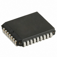
... Package Diagrams Document #: 38-06011 Rev. *A 32-Lead Plastic Leaded Chip Carrier J65 32-Pin Rectangular Leadless Chip Carrier L55 MIL-STD-1835 C-12 CY7C460A/CY7C462A CY7C464A/CY7C466A 51-85002-B 51-80068 Page ...
Page 14
... The inclusion of Cypress Semiconductor products in life-support systems application implies that the manufacturer assumes all risk of such use and in doing so indemnifies Cypress Semiconductor against all charges. 28-Lead (600-Mil) Molded DIP P15 28-Lead (300-Mil) Molded DIP P21 CY7C460A/CY7C462A CY7C464A/CY7C466A 51-85017-A 51-85014-B ...
Page 15
... Document Title: CY7C460A, CY7C462A, CY7C646A, CY7C466A Asynchronous, Cascadable 8K/16K/32K/64K X 9 FIFOs Document Number: 38-06011 Issue REV. ECN NO. Date ** 106472 09/10/01 *A 122263 12/26/02 Document #: 38-06011 Rev. *A Orig. of Change Description of Change SZV Change from Spec number 38-00627 to 38-06011 RBI Power up requirements added to Maximum Ratings Information ...