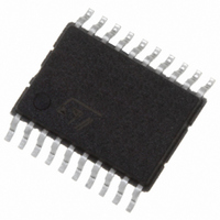
74LVC374ATTR STMicroelectronics, 74LVC374ATTR Datasheet

74LVC374ATTR
Specifications of 74LVC374ATTR
74LVC374ATTR
Available stocks
Related parts for 74LVC374ATTR
74LVC374ATTR Summary of contents
Page 1
... This device can be used to interface 5V to 3V. All inputs and outputs are equipped with protection circuits against static discharge, giving them 2KV ESD immunity and transient excess voltage. 74LVC374A HIGH PERFORMANCE SOP TSSOP PACKAGE T & R SOP 74LVC374AMTR TSSOP 74LVC374ATTR Rev. 2 1/14 ...
Page 2
Figure 2: Input And Output Equivalent Circuit Table 2: Pin Description PIN N° 12, 15, 16, 13, 14, 17 Table 3: Truth Table ...
Page 3
Table 4: Absolute Maximum Ratings Symbol V Supply Voltage Input Voltage Output Voltage ( Output Voltage (High or Low State) (note Input Diode Current ...
Page 4
Table 6: DC Specifications Symbol Parameter V High Level Input IH Voltage V Low Level Input IL Voltage V High Level Output OH Voltage V Low Level Output OL Voltage I Input Leakage I Current I Power Off Leakage ...
Page 5
Table 8: AC Electrical Characteristics Symbol Parameter t t Propagation Delay PLH PHL Time Propagation Delay PLH PHL Time Output Enable Time 1.65 to 1.95 PZL PZH t t Output ...
Page 6
Figure 3: Test Circuit pulse generator (typically OUT Table 10: Test Circuit And Waveform Symbol Value Symbol 1.65 to 1.95V C 30pF 1000 ...
Page 7
Figure 4: Waveform - Propagation Delay, Setup And Hold Times (f=1MHz; 50% duty cycle) Figure 5: Waveform - Output Enable And Disable Times (f=1MHz; 50% duty cycle) 74LVC374A 7/14 ...
Page 8
Figure 6: Waveform - Propagation Delay Time (f=1MHz; 50% duty cycle) 8/14 ...
Page 9
SO-20 MECHANICAL DATA DIM. MIN. A 2.35 A1 0.1 B 0.33 C 0.23 D 12. 10.00 h 0.25 L 0.4 k 0° ddd mm. TYP MAX. 2.65 0.093 0.30 0.004 0.51 0.013 0.32 0.009 13.00 0.496 ...
Page 10
DIM. MIN 0.05 A2 0.8 b 0.19 c 0.09 D 6.4 E 6 0˚ PIN 1 IDENTIFICATION 1 10/14 TSSOP20 MECHANICAL DATA mm. TYP MAX. 1.2 0.15 ...
Page 11
Tape & Reel SO-20 MECHANICAL DATA DIM. MIN 12 10.8 Bo 13.2 Ko 3.1 Po 3.9 P 11.9 mm. TYP MAX. 330 13.2 0.504 0.795 2.362 30.4 11 0.425 13.4 0.520 3.3 ...
Page 12
Tape & Reel TSSOP20 MECHANICAL DATA DIM. MIN 12 6.8 Bo 6.9 Ko 1.7 Po 3.9 P 11.9 12/14 mm. TYP MAX. 330 13.2 0.504 0.795 2.362 22.4 7 0.268 7.1 ...
Page 13
Table 11: Revision History Date Revision 21-May-2004 1 26-Jul-2004 2 Description of Changes First Release. Ordering Codes Revision - pag. 1. 74LVC374A 13/14 ...
Page 14
... No license is granted by implication or otherwise under any patent or patent rights of STMicroelectronics. Specifications mentioned in this publication are subject to change without notice. This publication supersedes and replaces all information previously supplied. STMicroelectronics products are not authorized for use as critical components in life support devices or systems without express written approval of STMicroelectronics ...


