MC74HCT273ADWG ON Semiconductor, MC74HCT273ADWG Datasheet - Page 3
MC74HCT273ADWG
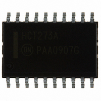
Manufacturer Part Number
MC74HCT273ADWG
Description
IC FLIP FLOP OCTAL D 20-SOIC
Manufacturer
ON Semiconductor
Series
74HCTr
Type
D-Type Busr
Datasheet
1.MC74HCT273ADTR2G.pdf
(8 pages)
Specifications of MC74HCT273ADWG
Function
Reset
Output Type
Non-Inverted
Number Of Elements
1
Number Of Bits Per Element
8
Frequency - Clock
30MHz
Delay Time - Propagation
25ns
Trigger Type
Positive Edge
Current - Output High, Low
4mA, 4mA
Voltage - Supply
4.5 V ~ 5.5 V
Operating Temperature
-55°C ~ 125°C
Mounting Type
Surface Mount
Package / Case
20-SOIC (7.5mm Width)
Logic Family
HCT
Technology
CMOS
Number Of Bits
8
Number Of Elements
1
Clock-edge Trigger Type
Positive-Edge
Polarity
Non-Inverting
Operating Supply Voltage (typ)
5V
Package Type
SOIC W
Propagation Delay Time
35ns
Low Level Output Current
4mA
High Level Output Current
-4mA
Operating Supply Voltage (min)
4.5V
Operating Supply Voltage (max)
5.5V
Operating Temp Range
-55C to 125C
Operating Temperature Classification
Military
Mounting
Surface Mount
Pin Count
20
Number Of Circuits
8
Logic Type
D-Type Flip-Flop
Input Type
Single-Ended
Supply Voltage (max)
5.5 V
Maximum Operating Temperature
+ 125 C
Mounting Style
SMD/SMT
Minimum Operating Temperature
- 55 C
Supply Voltage (min)
4.5 V
Lead Free Status / RoHS Status
Lead free / RoHS Compliant
Other names
MC74HCT273ADWG
MC74HCT273ADWGOS
MC74HCT273ADWGOS


Î Î Î Î
Î Î Î Î
Î Î Î Î
Î Î Î Î
Î Î Î Î
Î Î Î Î
Î Î Î Î
Î Î Î Î
Î Î Î Î
Î Î Î Î
Î Î Î Î
Î Î Î Î
Î Î Î Î
Î Î Î Î
Î Î Î Î
Î Î Î Î
Î Î Î Î
Î Î Î Î
Î Î Î Î
Î Î Î Î
Î Î Î Î
Î Î Î Î
Î Î Î Î
Î Î Î Î
Î Î Î Î
Î Î Î Î
Î Î Î Î
Î Î Î Î Î
Î Î Î Î Î
Î Î Î Î Î
Î Î Î Î Î
Î Î Î Î Î
Î Î Î Î Î
Î Î Î Î Î
Î Î Î Î Î
Î Î Î Î Î
Î Î Î Î Î
Î Î Î Î Î
Î Î Î Î Î
Î Î Î Î Î
NOTE: Information on typical parametric values can be found in Chapter 2 of the ON Semiconductor High−Speed CMOS Data Book
NOTE: For propagation delays with loads other than 50 pF, and information on typical parametric values, see Chapter 2 of the ON
* Used to determine the no−load dynamic power consumption: P
DC ELECTRICAL CHARACTERISTICS
AC ELECTRICAL CHARACTERISTICS
ON Semiconductor High−Speed CMOS Data Book (DL129/D).
Symbol
Symbol
ΔI
V
V
t
t
V
I
f
t
t
t
C
V
PLH
TLH
I
CC
max
PHL
PHL
THL
OH
OL
in
CC
IH
IL
PD
(DL129/D).
Semiconductor High−Speed CMOS Data Book (DL129/D).
,
,
Î Î Î Î Î Î Î Î Î
Î Î Î Î Î Î Î Î Î
Î Î Î Î Î Î Î Î Î
Î Î Î Î Î Î Î Î Î
Î Î Î Î Î Î Î Î Î
Î Î Î Î Î Î Î Î Î
Î Î Î Î Î Î Î Î Î
Î Î Î Î Î Î Î Î Î
Î Î Î Î Î Î Î Î Î
Î Î Î Î Î Î Î Î Î
Î Î Î Î Î Î Î Î Î
Î Î Î Î Î Î Î Î Î
Î Î Î Î Î Î Î Î Î
Î Î Î Î Î Î Î Î Î
Î Î Î Î Î Î Î Î Î
Î Î Î Î Î Î Î Î Î
Î Î Î Î Î Î Î Î Î
Î Î Î Î Î Î Î Î Î
Î Î Î Î Î Î Î Î Î
Î Î Î Î Î Î Î Î Î
Î Î Î Î Î Î Î Î Î
Î Î Î Î Î Î Î Î Î
Î Î Î Î Î Î Î Î Î
Î Î Î Î Î Î Î Î Î
Î Î Î Î Î Î Î Î Î
Î Î Î Î Î Î Î Î Î
Î Î Î Î Î Î Î Î Î
Î Î Î Î Î Î Î Î Î Î Î Î Î Î Î Î
Î Î Î Î Î Î Î Î Î Î Î Î Î Î Î Î
Î Î Î Î Î Î Î Î Î Î Î Î Î Î Î Î
Î Î Î Î Î Î Î Î Î Î Î Î Î Î Î Î
Î Î Î Î Î Î Î Î Î Î Î Î Î Î Î Î
Î Î Î Î Î Î Î Î Î Î Î Î Î Î Î Î
Î Î Î Î Î Î Î Î Î Î Î Î Î Î Î Î
Î Î Î Î Î Î Î Î Î Î Î Î Î Î Î Î
Î Î Î Î Î Î Î Î Î Î Î Î Î Î Î Î
Î Î Î Î Î Î Î Î Î Î Î Î Î Î Î Î
Î Î Î Î Î Î Î Î Î Î Î Î Î Î Î Î
Î Î Î Î Î Î Î Î Î Î Î Î Î Î Î Î
Î Î Î Î Î Î Î Î Î Î Î Î Î Î Î Î
Minimum High−Level Input
Voltage
Maximum Low−Level Input
Voltage
Minimum High−Level Output
Voltage
Maximum Low−Level Output
Voltage
Maximum Input Leakage
Current
Maximum Quiescent Supply
Current (per Package)
Additional Quiescent Supply
Current
Power Dissipation Capacitance (Per Gate)*
Maximum Clock Frequency (50% Duty Cycle)
Maximum Propagation Delay, Clock to Q
Maximum Propagation Delay, Reset to Q
Maximum Output Transition Time, Any Output
Parameter
Parameter
Î Î Î Î Î Î Î Î Î
Î Î Î Î Î Î Î Î Î
Î Î Î Î Î Î Î Î Î
Î Î Î Î Î Î Î Î Î
Î Î Î Î Î Î Î Î Î
Î Î Î Î Î Î Î Î Î
Î Î Î Î Î Î Î Î Î
Î Î Î Î Î Î Î Î Î
Î Î Î Î Î Î Î Î Î
Î Î Î Î Î Î Î Î Î
Î Î Î Î Î Î Î Î Î
Î Î Î Î Î Î Î Î Î
Î Î Î Î Î Î Î Î Î
Î Î Î Î Î Î Î Î Î
Î Î Î Î Î Î Î Î Î
Î Î Î Î Î Î Î Î Î
Î Î Î Î Î Î Î Î Î
Î Î Î Î Î Î Î Î Î
Î Î Î Î Î Î Î Î Î
Î Î Î Î Î Î Î Î Î
Î Î Î Î Î Î Î Î Î
Î Î Î Î Î Î Î Î Î
Î Î Î Î Î Î Î Î Î
Î Î Î Î Î Î Î Î Î
Î Î Î Î Î Î Î Î Î
Î Î Î Î Î Î Î Î Î
Î Î Î Î Î Î Î Î Î
Î Î Î Î Î Î Î Î Î
Î Î Î Î Î Î Î Î Î
(Voltages Referenced to GND)
(V
V
|I
V
|I
V
|I
V
|I
V
|I
V
|I
V
V
I
V
V
l
out
out
out
out
out
out
out
out
out
out
CC
in
in
in
in
in
in
in
in
= V
= V
= V
= V
= V
= V
= 2.4 V, Any One Input
= V
| v 20 μA
| v 20 μA
| v 20 μA
| v 4.0 mA
| v 20 μA
| v 4.0 mA
= 0 μA
= 0 μA
= 0.1 V or V
= 0.1 V or V
= 5.0 V ± 10%, C
IH
IH
IH
IH
CC
CC
CC
Test Conditions
or V
or V
or V
or V
or GND
or GND
or GND, Other Inputs
http://onsemi.com
IL
IL
IL
IL
CC
CC
D
– 0.1 V
– 0.1 V
= C
3
L
= 50 pF, Input t
PD
V
CC
Î Î Î Î
Î Î Î Î
Î Î Î Î
Î Î Î Î
Î Î Î Î
Î Î Î Î
Î Î Î Î
Î Î Î Î
Î Î Î Î
Î Î Î Î
Î Î Î Î
Î Î Î Î
Î Î Î Î
Î Î Î Î
Î Î Î Î
Î Î Î Î
Î Î Î Î
Î Î Î Î
Î Î Î Î
Î Î Î Î
Î Î Î Î
Î Î Î Î
Î Î Î Î
Î Î Î Î
Î Î Î Î
Î Î Î Î
Î Î Î Î
Î Î Î Î
Î Î Î Î
Î Î Î Î
Î Î Î Î
Î Î Î Î
Î Î Î Î
Î Î Î Î
Î Î Î Î
Î Î Î Î
Î Î Î Î
Î Î Î Î
Î Î Î Î
Î Î Î Î
Î Î Î Î
Î Î Î Î
2
f + I
CC
V
Fig.
1, 4
1, 4
2, 4
1, 5
4.5
5.5
4.5
5.5
4.5
5.5
4.5
4.5
5.5
4.5
5.5
5.5
5.5
r
V
CC
= t
V
CC
f
= 6.0 ns)
Î Î Î Î Î Î Î Î Î
Î Î Î Î Î Î Î Î Î
Î Î Î Î
Î Î Î Î
Î Î Î Î
Î Î Î Î
Î Î Î Î
Î Î Î Î
Î Î Î Î
Î Î Î Î
Î Î Î Î
Î Î Î Î
Î Î Î Î
Î Î Î Î
Î Î Î Î
Î Î Î Î
Î Î Î Î
Î Î Î Î
Î Î Î Î
Î Î Î Î
Î Î Î Î
Î Î Î Î
Î Î Î Î
Î Î Î Î
Î Î Î Î
Î Î Î Î
Î Î Î Î
Î Î Î Î
Î Î Î Î
Î Î Î Î
Î Î Î Î
Î Î Î Î Î Î Î Î Î
Î Î Î Î Î Î Î Î Î
Î Î Î Î
Î Î Î Î
Î Î Î Î
Î Î Î Î
Î Î Î Î
Î Î Î Î
Î Î Î Î
Î Î Î Î
Î Î Î Î
Î Î Î Î
Î Î Î Î
Î Î Î Î
. For load considerations, see Chapter 2 of the
≥ −55_C
– 55 to
– 55 to
25_C
25_C
Typical @ 25°C, V
± 0.1
3.98
0.26
2.0
2.0
0.8
0.8
4.4
5.4
0.1
0.1
4.0
2.9
30
25
25
18
Guaranteed Limit
Guaranteed Limit
Î Î Î
Î Î Î
Î Î Î
Î Î Î
Î Î Î
Î Î Î
Î Î Î
Î Î Î
Î Î Î
Î Î Î
Î Î Î
Î Î Î
Î Î Î
Î Î Î
Î Î Î
Î Î Î
Î Î Î
Î Î Î
Î Î Î
Î Î Î
Î Î Î
Î Î Î
Î Î Î
Î Î Î
Î Î Î Î Î Î
Î Î Î Î Î Î
Î Î Î Î Î Î
Î Î Î Î Î Î
Î Î Î Î Î Î
Î Î Î
Î Î Î
Î Î Î
Î Î Î
Î Î Î
Î Î Î
Î Î Î
Î Î Î
Î Î Î
Î Î Î
Î Î Î
Î Î Î
v 85_C
v 85_C
± 1.0
3.84
0.33
2.0
2.0
0.8
0.8
4.4
5.4
0.1
0.1
25_C to 125_C
40
24
28
28
20
30
Î Î Î Î
Î Î Î Î
Î Î Î Î
Î Î Î Î
Î Î Î Î
Î Î Î Î
Î Î Î Î
Î Î Î Î
Î Î Î Î
Î Î Î Î
Î Î Î Î
Î Î Î Î
Î Î Î Î
Î Î Î Î
Î Î Î Î
Î Î Î Î
Î Î Î Î
Î Î Î Î
Î Î Î Î
Î Î Î Î
Î Î Î Î
Î Î Î Î
Î Î Î Î
Î Î Î Î
Î Î Î Î
Î Î Î Î
Î Î Î Î
Î Î Î Î
Î Î Î Î
Î Î Î Î
Î Î Î Î
Î Î Î Î
Î Î Î Î
Î Î Î Î
Î Î Î Î
Î Î Î Î
CC
2.4
v 125_C
v 125_C
= 5.0 V
± 1.0
160
2.0
2.0
0.8
0.8
4.4
5.4
3.7
0.1
0.1
0.4
20
35
35
22
Î Î Î
Î Î Î
Î Î Î
Î Î Î
Î Î Î
Î Î Î
Î Î Î
Î Î Î
Î Î Î
Î Î Î
Î Î Î
Î Î Î
Î Î Î
Î Î Î
Î Î Î
Î Î Î
Î Î Î
Î Î Î
Î Î Î
Î Î Î
Î Î Î
Î Î Î
Î Î Î
Î Î Î
Î Î Î
Î Î Î
Î Î Î
Î Î Î
Î Î Î
Î Î Î
Î Î Î
Î Î Î
Î Î Î
Î Î Î
Î Î Î
Î Î Î
Î Î Î
Î Î Î
Î Î Î
Î Î Î
MHz
Unit
Unit
mA
μA
μA
ns
ns
ns
pF
V
V
V
V
Related parts for MC74HCT273ADWG
Image
Part Number
Description
Manufacturer
Datasheet
Request
R

Part Number:
Description:
ON Semiconductor [VOLTAGE REGULATOR]
Manufacturer:
ON Semiconductor
Datasheet:
Part Number:
Description:
357-036-542-201 CARDEDGE 36POS DL .156 BLK LOPRO
Manufacturer:
ON Semiconductor
Datasheet:
Part Number:
Description:
357-036-542-201 CARDEDGE 36POS DL .156 BLK LOPRO
Manufacturer:
ON Semiconductor
Datasheet:
Part Number:
Description:
357-036-542-201 CARDEDGE 36POS DL .156 BLK LOPRO
Manufacturer:
ON Semiconductor
Datasheet:
Part Number:
Description:
357-036-542-201 CARDEDGE 36POS DL .156 BLK LOPRO
Manufacturer:
ON Semiconductor
Datasheet:
Part Number:
Description:
357-036-542-201 CARDEDGE 36POS DL .156 BLK LOPRO
Manufacturer:
ON Semiconductor
Datasheet:
Part Number:
Description:
357-036-542-201 CARDEDGE 36POS DL .156 BLK LOPRO
Manufacturer:
ON Semiconductor
Datasheet:
Part Number:
Description:
357-036-542-201 CARDEDGE 36POS DL .156 BLK LOPRO
Manufacturer:
ON Semiconductor
Datasheet:
Part Number:
Description:
357-036-542-201 CARDEDGE 36POS DL .156 BLK LOPRO
Manufacturer:
ON Semiconductor
Datasheet:
Part Number:
Description:
357-036-542-201 CARDEDGE 36POS DL .156 BLK LOPRO
Manufacturer:
ON Semiconductor
Datasheet:
Part Number:
Description:
357-036-542-201 CARDEDGE 36POS DL .156 BLK LOPRO
Manufacturer:
ON Semiconductor
Datasheet:
Part Number:
Description:
Manufacturer:
ON Semiconductor
Datasheet:
Part Number:
Description:
Manufacturer:
ON Semiconductor
Datasheet:
Part Number:
Description:
Manufacturer:
ON Semiconductor
Datasheet: