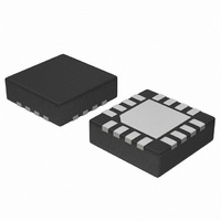
NB4L52MNG ON Semiconductor, NB4L52MNG Datasheet - Page 7

NB4L52MNG
Manufacturer Part Number
NB4L52MNG
Description
IC FLIP FLOP DATA/CLK DFF 16-QFN
Manufacturer
ON Semiconductor
Type
D-Typer
Datasheet
1.NB4L52MNR2G.pdf
(8 pages)
Specifications of NB4L52MNG
Function
Reset
Output Type
Differential
Number Of Elements
1
Number Of Bits Per Element
1
Delay Time - Propagation
400ps
Trigger Type
Negative Edge
Voltage - Supply
2.3 V ~ 5.5 V
Operating Temperature
-40°C ~ 85°C
Mounting Type
Surface Mount
Package / Case
16-TQFN Exposed Pad
Logic Type
Registered Translator
Translation
CML/ECL/LVCMOS/LVDS/LVTTL to LVPECL
Propagation Delay Time
0.5 ns
Supply Voltage (max)
- 5.5 V, + 5.5 V
Supply Voltage (min)
- 2.375 V, + 2.375 V
Maximum Operating Temperature
+ 85 C
Minimum Operating Temperature
- 40 C
Mounting Style
SMD/SMT
Flip-flop Type
D
Propagation Delay
330ps
Frequency
4GHz
Output Current
25mA
Ic Output Type
Differential / Complementary
Supply Voltage Range
± 2.375V To ± 5.5V
Rohs Compliant
Yes
Lead Free Status / RoHS Status
Lead free / RoHS Compliant
Current - Output High, Low
-
Frequency - Clock
-
Lead Free Status / Rohs Status
Lead free / RoHS Compliant
Available stocks
Company
Part Number
Manufacturer
Quantity
Price
Company:
Part Number:
NB4L52MNG
Manufacturer:
ON Semiconductor
Quantity:
2
†For information on tape and reel specifications, including part orientation and tape sizes, please refer to our Tape and Reel Packaging
ORDERING INFORMATION
Specifications Brochure, BRD8011/D.
NB4L52MNG
NB4L52MNR2G
Device
(See Application Note AND8020/D − Termination of ECL Logic Devices.)
Figure 10. Typical Termination for Output Driver and Device Evaluation
Driver
Device
NB6L239
QFN−16, 3 x 3 mm
QFN−16, 3 x 3 mm
(Pb−Free)
(Pb−Free)
Package
Q
Q
Resource Reference of Application Notes
AN1405/D
AN1406/D
AN1503/D
AN1504/D
AN1568/D
AN1672/D
AND8001/D − Odd Number Counters Design
AND8002/D − Marking and Date Codes
AND8020/D − Termination of ECL Logic Devices
AND8066/D − Interfacing with ECLinPS
AND8090/D − AC Characteristics of ECL Devices
− ECL Clock Distribution Techniques
− Designing with PECL (ECL at +5.0 V)
− ECLinPS I/O SPiCE Modeling Kit
− Metastability and the ECLinPS Family
− Interfacing Between LVDS and ECL
− The ECL Translator Guide
Z
Z
http://onsemi.com
o
o
= 50 W
= 50 W
50 W
V
7
TT
= V
V
CC
TT
− 2.0 V
50 W
3000 / Tape & Reel
123 Units / Rail
Shipping
D
D
Receiver
Device
†


