NB7V52MMNTXG ON Semiconductor, NB7V52MMNTXG Datasheet
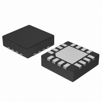
IC FLIP FLOP DIFF RST/CML 16-QFN

NB7V52MMNTXG

Manufacturer Part Number
NB7V52MMNTXG
Description
IC FLIP FLOP DIFF RST/CML 16-QFN
Manufacturer
ON Semiconductor
Type
D-Typer
Datasheet

Specifications of NB7V52MMNTXG

Function
Reset
Output Type
Differential
Number Of Elements
1
Number Of Bits Per Element
1
Delay Time - Propagation
300ps
Trigger Type
Negative Edge
Operating Temperature
-40°C ~ 85°C
Mounting Type
Surface Mount
Package / Case
16-TQFN Exposed Pad
Lead Free Status / RoHS Status
Lead free / RoHS Compliant
Voltage - Supply
-
Current - Output High, Low
-
Frequency - Clock
-
NB7V52M
1.8V / 2.5V Differential D
Flip-Flop w/ Reset and CML
Outputs
Multi−Level Inputs w/ Internal Termination
Description
differential asynchronous Reset. The differential D/D, CLK/CLK and
R/R inputs incorporate dual internal 50 W termination resistors and
will accept LVPECL, CML, LVDS logic levels.
transferred to the differential CML outputs. The differential Clock
inputs allow the NB7V52M to also be used as a negative edge
triggered device.
50 W termination and produce 400 mV output swings when externally
receiver terminated with a 50 W resistor to V
QFN package. The NB7V52M is a member of the GigaComm™
family of high performance clock products. Application notes,
m o d e l s , a n d s u p p o r t d o c u m e n t a t i o n a r e a v a i l a b l e a t
www.onsemi.com.
Features
© Semiconductor Components Industries, LLC, 2009
September, 2009 − Rev. 3
The NB7V52M is a 10 GHz differential D flip−flop with a
When Clock transitions from logic Low to High, Data will be
The 16 mA differential CML outputs provide matching internal
The NB7V52M is offered in a low profile 3 mm x 3 mm 16−pin
Maximum Input Clock Frequency > 10 GHz
Maximum Input Data Rate > 10 Gb/s
Random Clock Jitter < 0.8 ps RMS, Max
200 ps Typical Propagation Delay
35 ps Typical Rise and Fall Times
Differential CML Outputs, 400 mV Peak−to−Peak, Typical
Operating Range: V
Internal 50 W Input Termination Resistors
QFN−16 Package, 3mm x 3mm
−40°C to +85°C Ambient Operating Temperature
These are Pb−Free Devices
CC
= 1.71 V to 2.625 V with V
CC
.
EE
= 0 V
1
See detailed ordering and shipping information in the package
dimensions section on page 9 of this data sheet.
VTCLK
VTCLK
*For additional marking information, refer to
CASE 485G
MN SUFFIX
VTD
VTD
CLK
CLK
Application Note AND8002/D.
A
L
Y
W
G
(Note: Microdot may be in either location)
QFN−16
D
D
1
ORDERING INFORMATION
Figure 1. Logic Diagram
= Assembly Location
= Wafer Lot
= Year
= Work Week
= Pb−Free Package
http://onsemi.com
VTR
D Flip−Flop
RESET
Publication Order Number:
R
1
DIAGRAM*
R
MARKING
16
ALYWG
NB7V
52M
VTR
G
NB7V52M/D
Q
Q

Related parts for NB7V52MMNTXG

NB7V52MMNTXG Summary of contents

Page 1

NB7V52M 1.8V / 2.5V Differential D Flip-Flop w/ Reset and CML Outputs Multi−Level Inputs w/ Internal Termination Description The NB7V52M GHz differential D flip−flop with a differential asynchronous Reset. The differential D/D, CLK/CLK and R/R inputs incorporate ...

Page 2

VTR R R VTR VTD NB7V52M D 3 VTD VTCLK CLK CLK VTCLK Figure 2. Pin Configuration (Top View) Table 1. Pin Description Pin Name I/O 1 VTD ...

Page 3

Table 2. ATTRIBUTES ESD Protection Moisture Sensitivity Flammability Rating Transistor Count Meets or exceeds JEDEC Spec EIA/JESD78 IC Latchup Test For additional information, see Application Note AND8003/D. Table 3. MAXIMUM RATINGS Symbol Parameter V Positive Power Supply CC V Positive ...

Page 4

Table 4. DC CHARACTERISTICS, Multi−Level Inputs Symbol Characteristic POWER SUPPLY CURRENT I Power Supply Current (Inputs and Outputs Open) CC CML OUTPUTS V Output HIGH Voltage (Note Output LOW Voltage (Note 5) OL DIFFERENTIAL CLOCK INPUTS DRIVEN ...

Page 5

Table 5. AC CHARACTERISTICS V Symbol f Maximum Input Clock Frequency MAX f Maximum Input Data Rate (PRBS23) DATA MAX V Output Voltage Amplitude (@ V OUTPP (See Figures 3 and 10, Note 11 Propagation Delay to Differential ...

Page 6

V CLK CLK V th Figure 5. Differential Input Driven Single−Ended IHmax V thmax V ILmax CLK IHmin V thmin V ILmin V ...

Page 7

NB7V52M TOUT TOUT Figure 11. Typical CML Output Structure and Termination DUT Driver Device Q Figure 12. ...

Page 8

LVPECL TD V Driver − GND/V EE Figure 13. LVPECL Interface V CML Driver GND Figure 15. ...

Page 9

... ORDERING INFORMATION Device NB7V52MMNG NB7V52MMNHTBG NB7V52MMNTXG †For information on tape and reel specifications, including part orientation and tape sizes, please refer to our Tape and Reel Packaging Specifications Brochure, BRD8011/D. Package QFN−16 (Pb−free) QFN−16 (Pb−free) QFN−16 (Pb−free) http://onsemi.com 9 † ...

Page 10

... E2 e 3.25 0.128 *For additional information on our Pb−Free strategy and soldering details, please download the ON Semiconductor Soldering and Mounting Techniques Reference Manual, SOLDERRM/D. 6,362,644. N. American Technical Support: 800−282−9855 Toll Free USA/Canada Japan: ON Semiconductor, Japan Customer Focus Center 2−9−1 Kamimeguro, Meguro−ku, Tokyo, Japan 153−0051 Phone: 81− ...

Related keywords