NBSG53ABA ON Semiconductor, NBSG53ABA Datasheet - Page 5
NBSG53ABA
Manufacturer Part Number
NBSG53ABA
Description
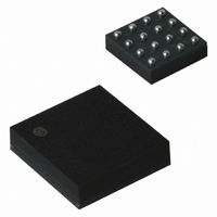
IC FLIP FLOP DIFF CLOCK 16FCBGA
Manufacturer
ON Semiconductor
Type
D-Type Busr
Datasheet
1.NBSG53ABA.pdf
(18 pages)
Specifications of NBSG53ABA
Function
Reset
Output Type
Differential
Number Of Elements
1
Number Of Bits Per Element
2
Frequency - Clock
8GHz
Trigger Type
Positive, Negative
Voltage - Supply
2.375 V ~ 3.465 V
Operating Temperature
-40°C ~ 85°C
Mounting Type
Surface Mount
Package / Case
16-FCBGA
Lead Free Status / RoHS Status
Contains lead / RoHS non-compliant
Current - Output High, Low
-
Delay Time - Propagation
-
Other names
NBSG53ABAOS
Available stocks
Company
Part Number
Manufacturer
Quantity
Price

Company:
Part Number:
NBSG53ABAHTBG
Manufacturer:
ON Semiconductor
Quantity:
10 000
Company:
Part Number:
NBSG53ABAR2
Manufacturer:
ON Semiconductor
Quantity:
10 000


NOTE: GigaComm circuits are designed to meet the DC specifications shown in the above table after thermal equilibrium has been established.
9. Input and output parameters vary 1:1 with V
10. All outputs loaded with 50 W to V
11. V
12. V
13. V
14. V
*Typicals used for testing purposes.
**The device packaged in FCBGA-16 have maximum ambient temperature specification of 70 C and devices packaged in QFN-16 have
Table 7. DC CHARACTERISTICS, INPUT WITH PECL OUTPUT
Symbol
maximum ambient temperature specification of 85 C.
I
V
V
V
V
V
V
V
V
V
R
I
I
EE
IH
IL
OH
OL
OUTPP
IH
IL
IH
IL
THR
IHCMR
TIN
input signal.
IHCMR
IH
IL
THR
always w V
cannot exceed V
The circuit is in a test socket or mounted on a printed circuit board and transverse airflow greater than 500 lfpm is maintained.
is the voltage applied to one input when running in single-ended mode.
min varies 1:1 with V
Negative Power Supply Current
Output HIGH Voltage (Note 10)
Output LOW Voltage (Note 10)
Output Voltage Amplitude
Input HIGH Voltage (Single-Ended)
(Notes 12 and 14)
Input LOW Voltage (Single-Ended)
(Notes 13 and 14)
Input High Voltage (Single-Ended)
Input Low Voltage (Single-Ended)
Input Threshold Voltage (Single-Ended)
(Note 14)
Input HIGH Voltage Common Mode
Range (Differential Configuration)
(Note 11)
Internal Input Termination Resistor
Input HIGH Current (@V
Input LOW Current (@V
(OLS = V
(OLS = V
EE
. |V
CC
Characteristic
IL
CC
CC
. |V
- V
- 0.8 V, OLS = FLOAT)
- 0.8 V, OLS = FLOAT)
IH
THR
EE
(OLS = V
(OLS = V
(OLS = V
(OLS = V
- V
, V
| < 2600 mV.
CC
THR
IL
IHCMR
IH
CLK, CLK, D, D
CLK, CLK, D, D
CLK, CLK, D, D
CLK, CLK, D, D
)
)
- 2.0 V.
| < 2600 mV.
(OLS = V
(OLS = V
(OLS = V
(OLS = V
CC
CC
CC
CC
max varies 1:1 with V
- 0.4 V)
- 1.2 V)
- 0.4 V)
- 1.2 V)
R, SEL
R, SEL
R, SEL
R, SEL
CC
CC
CC
EE
EE
. V
)
)
)
)
EE
V
V
1460
1235
1455
1005
1275
1290
1125
can vary +0.125 V to -0.965 V.
Min
V
V
555
775
715
125
525
325
1.2
EE
33
45
EE
0
EE
EE
http://onsemi.com
+
+
NBSG53A
-40 C
V
1000*
1400*
CC
V
1510
1295
1505
1095
Typ
705
895
805
215
615
415
CC
45
CC
50
35
20
5
5
5
. The V
-
-
5
V
1560
1355
1015
1555
1185
Max
V
V
V
855
150
890
100
100
IHCMR
2.5
57
CC
75
55
50
50
IH
CC
CC
V
-
-
CC
range is referenced to the most positive side of the differential
= 2.5 V; V
V
V
1490
1270
1490
1040
1275
1355
1125
Min
V
V
595
810
705
120
520
320
EE
1.2
33
45
EE
0
EE
EE
+
+
V
1000*
1400*
V
25 C
1540
1330
1540
1130
EE
Typ
745
930
795
210
610
410
CC
45
CC
50
35
20
0
5
5
= 0 V (Note 9)
-
-
V
1590
1390
1050
1590
1220
V
Max
V
V
895
150
955
100
100
2.5
57
75
55
50
50
CC
IH
CC
CC
-
-
70 C(BGA)/85 C(QFN)**
V
V
1515
1295
1510
1065
1275
1415
1125
Min
625
840
700
120
515
320
V
V
1.2
EE
33
45
EE
0
EE
EE
+
+
1000*
1400*
V
V
1565
1355
1560
1155
Typ
775
960
790
210
605
410
45
50
35
20
CC
CC
5
5
5
-
-
V
1615
1415
1080
1610
1245
1015
Max
V
V
V
925
150
100
100
2.5
57
CC
75
55
50
50
IH
CC
CC
-
-
Unit
mA
mV
mV
mV
mV
mV
mV
mV
mV
mA
mA
W
V
Related parts for NBSG53ABA
Image
Part Number
Description
Manufacturer
Datasheet
Request
R

Part Number:
Description:
ON Semiconductor [VOLTAGE REGULATOR]
Manufacturer:
ON Semiconductor
Datasheet:
Part Number:
Description:
357-036-542-201 CARDEDGE 36POS DL .156 BLK LOPRO
Manufacturer:
ON Semiconductor
Datasheet:
Part Number:
Description:
357-036-542-201 CARDEDGE 36POS DL .156 BLK LOPRO
Manufacturer:
ON Semiconductor
Datasheet:
Part Number:
Description:
357-036-542-201 CARDEDGE 36POS DL .156 BLK LOPRO
Manufacturer:
ON Semiconductor
Datasheet:
Part Number:
Description:
357-036-542-201 CARDEDGE 36POS DL .156 BLK LOPRO
Manufacturer:
ON Semiconductor
Datasheet:
Part Number:
Description:
357-036-542-201 CARDEDGE 36POS DL .156 BLK LOPRO
Manufacturer:
ON Semiconductor
Datasheet:
Part Number:
Description:
357-036-542-201 CARDEDGE 36POS DL .156 BLK LOPRO
Manufacturer:
ON Semiconductor
Datasheet:
Part Number:
Description:
357-036-542-201 CARDEDGE 36POS DL .156 BLK LOPRO
Manufacturer:
ON Semiconductor
Datasheet:
Part Number:
Description:
357-036-542-201 CARDEDGE 36POS DL .156 BLK LOPRO
Manufacturer:
ON Semiconductor
Datasheet:
Part Number:
Description:
357-036-542-201 CARDEDGE 36POS DL .156 BLK LOPRO
Manufacturer:
ON Semiconductor
Datasheet:
Part Number:
Description:
357-036-542-201 CARDEDGE 36POS DL .156 BLK LOPRO
Manufacturer:
ON Semiconductor
Datasheet:
Part Number:
Description:
Manufacturer:
ON Semiconductor
Datasheet:
Part Number:
Description:
Manufacturer:
ON Semiconductor
Datasheet:
Part Number:
Description:
Manufacturer:
ON Semiconductor
Datasheet: