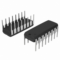
MC14049UBCPG ON Semiconductor, MC14049UBCPG Datasheet - Page 4

MC14049UBCPG
Manufacturer Part Number
MC14049UBCPG
Description
IC INVERTER HEX 1-INPUT 16DIP
Manufacturer
ON Semiconductor
Series
4000Br
Specifications of MC14049UBCPG
Logic Type
Inverter
Number Of Inputs
1
Number Of Circuits
6
Current - Output High, Low
3.75mA, 24mA
Voltage - Supply
3 V ~ 18 V
Operating Temperature
-55°C ~ 125°C
Mounting Type
Through Hole
Package / Case
16-DIP (0.300", 7.62mm)
Logic Family
MC140
Number Of Channels Per Chip
Hex
Polarity
Inverting
Supply Voltage (max)
18 V
Supply Voltage (min)
3 V
Maximum Operating Temperature
+ 125 C
Mounting Style
Through Hole
High Level Output Current
- 4.7 mA (Min)
Input Bias Current (max)
4 uA
Low Level Output Current
30 mA (Min)
Minimum Operating Temperature
- 55 C
Propagation Delay Time
120 ns @ 5 V or 65 ns @ 10 V or 50 ns @ 15 V
Current, Supply
120 μA
Function Type
6-Channels
Logic Function
Buffer
Package Type
PDIP-16
Special Features
Inverting
Temperature, Operating, Range
-55 to +125 °C
Voltage, Supply
3 to 18 VDC
Number Of Lines (input / Output)
6 / 6
Logic Device Type
Buffer, Inverting
Supply Voltage Range
3V To 18V
Logic Case Style
DIP
No. Of Pins
16
Operating Temperature Range
-55°C To +125°C
Filter Terminals
DIP
Rohs Compliant
Yes
Family Type
4000 CMOS
Lead Free Status / RoHS Status
Lead free / RoHS Compliant
Other names
MC14049UBCPGOS
Available stocks
Company
Part Number
Manufacturer
Quantity
Price
Part Number:
MC14049UBCPG
Manufacturer:
ON/安森美
Quantity:
20 000
−10
−20
−30
−40
−50
1000
1200
1100
700
800
740
600
500
400
300
200
100
900
825
0
−10
Figure 5. Typical Output Source Characteristics
0
V
25
Figure 7. Ambient Temperature Power Derating
GS
= 10 Vdc
V
GS
−8.0
V
50
T
= 15 Vdc
DS
(D) SOIC
A
, AMBIENT TEMPERATURE ( C)
, DRAIN−TO−SOURCE VOLTAGE (Vdc)
8
V
1
V
75
−6.0
DD
SS
V
GS
V
I
DS
OH
= 5.0 Vdc
100
= V
MAXIMUM CURRENT LEVEL
(P) PDIP
−4.0
OH
V
OH
− V
DD
125
−2.0
150
http://onsemi.com
MC14049UB
0
175
4
175 mW (P)
120 mW (D)
160
120
80
40
0
0
Figure 6. Typical Output Sink Characteristics
INPUT
20 ns
OUTPUT
GENERATOR
t
PULSE
PHL
Figure 8. Switching Time Test Circuit
2.0
V
DS
, DRAIN−TO−SOURCE VOLTAGE (Vdc)
V
GS
= 5.0 Vdc
8
90%
50%
10%
V
1
V
V
4.0
and Waveforms
DD
SS
MAXIMUM CURRENT LEVEL
in
90%
50%
10%
t
THL
8
I
OL
V
1
V
V
6.0
DD
SS
DD
V
= V
OL
OL
20 ns
V
V
8.0
GS
GS
t
C
PLH
= 15 Vdc
= 10 Vdc
L
t
TLH
V
out
V
V
V
V
SS
OH
OL
DD
10


