74HCT132N,652 NXP Semiconductors, 74HCT132N,652 Datasheet - Page 5
74HCT132N,652
Manufacturer Part Number
74HCT132N,652
Description
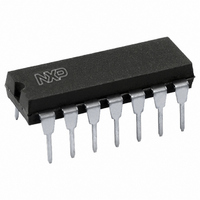
IC TRIGGER NAND QUAD 2IN 14DIP
Manufacturer
NXP Semiconductors
Series
74HCTr
Datasheets
1.74HCT4046ADB112.pdf
(19 pages)
2.74HCT4046ADB112.pdf
(23 pages)
3.74HC132N652.pdf
(8 pages)
Specifications of 74HCT132N,652
Number Of Circuits
4
Package / Case
14-DIP (0.300", 7.62mm)
Logic Type
NAND Gate - Schmitt Trigger
Number Of Inputs
2
Current - Output High, Low
5.2mA, 5.2mA
Voltage - Supply
4.5 V ~ 5.5 V
Operating Temperature
-40°C ~ 125°C
Mounting Type
Through Hole
Product
NAND
Logic Family
74HCT
High Level Output Current
- 4 mA
Low Level Output Current
4 mA
Propagation Delay Time
17 ns
Supply Voltage (max)
5.5 V
Supply Voltage (min)
4.5 V
Maximum Operating Temperature
+ 125 C
Mounting Style
SMD/SMT
Minimum Operating Temperature
- 40 C
Logical Function
NAND
Number Of Elements
4
Operating Supply Voltage (typ)
5V
Operating Temp Range
-40C to 125C
Package Type
PDIP
Number Of Outputs
1
Technology
CMOS
Mounting
Through Hole
Pin Count
14
Operating Temperature Classification
Automotive
Quiescent Current
2uA
Operating Supply Voltage (max)
5.5V
Operating Supply Voltage (min)
4.5V
Lead Free Status / RoHS Status
Lead free / RoHS Compliant
Lead Free Status / RoHS Status
Lead free / RoHS Compliant, Lead free / RoHS Compliant
Other names
568-1511-5
74HCT132N
933669150652
74HCT132N
933669150652


Philips Semiconductors
DC CHARACTERISTICS FOR 74HCT
For the DC characteristics see
given below.
Output capability: standard
I
Notes to HCT types
The value of additional quiescent supply current ( I
To determine I
Transfer characteristics for 74HCT
Voltages are referenced to GND (ground = 0 V)
AC CHARACTERISTICS FOR 74HCT
GND = 0 V; t
September 1993
CC
INPUT
nA, nB
SYMBOL PARAMETER
V
V
V
SYMBOL PARAMETER
t
t
PHL
THL
T
T
H
Quad 2-input NAND Schmitt trigger
category: SSI
/ t
/ t
TLH
PLH
positive-going threshold
negative-going threshold 0.5
hysteresis (V
propagation delay
output transition time
r
nA, nB to nY
= t
UNIT LOAD COEFFICIENT
CC
f
= 6 ns; C
0.3
per input, multiply this value by the unit load coefficient shown in the table below.
T
L
= 50 pF
V
“74HC/HCT/HCU/HCMOS Logic Family Specifications”
T
)
min.
min. typ.
1.2
1.4
0.6
0.4
0.4
typ.
20
7
25
1.41
1.59
0.85
0.99
0.56
0.60
25
max. min.
CC
33
15
max. min. max.
1.9
2.1
1.2
1.4
) for a unit load of 1 is given in the family specifications.
T
74HCT
amb
T
5
40 to 85
1.2
1.4
0.5
0.6
0.4
0.4
74HCT
amb
( C)
40 to 85
( C)
max.
41
19
1.9
2.1
1.2
1.4
min.
40 to 125
min. max.
1.2
1.4
0.5
0.6
0.4
0.4
40 to 125
max.
2.1
1.4
1.9
1.2
50
22
. Transfer characteristics are
ns
ns
UNIT
V
V
V
UNIT
74HC/HCT132
V
(V)
4.5
4.5
TEST CONDITIONS
CC
TEST CONDITIONS
V
4.5
5.5
4.5
5.5
4.5
5.5
Product specification
(V)
CC
Fig.13
Fig.13
WAVEFORMS
WAVEFORMS
Figs 6 and 7
Figs 6 and 7
Figs 6 and 7
Related parts for 74HCT132N,652
Image
Part Number
Description
Manufacturer
Datasheet
Request
R

Part Number:
Description:
IC BUFF/DVR TRI-ST DUAL 20DIP
Manufacturer:
Fairchild Semiconductor
Datasheet:

Part Number:
Description:
IC BUS TRANSCVR 3-ST 8BIT 20DIP
Manufacturer:
ON Semiconductor
Datasheet:

Part Number:
Description:
IC TRANSCEIVER 3-ST 8BIT 20SOIC
Manufacturer:
Fairchild Semiconductor
Datasheet:

Part Number:
Description:
IC BUFFER NONINV QUAD 3ST 14SOIC
Manufacturer:
ON Semiconductor
Datasheet:
Part Number:
Description:
IC BUFFER NONINV QUAD 3ST 14SOIC
Manufacturer:
ON Semiconductor
Datasheet:

Part Number:
Description:
IC BUS TRANSCVR 3-ST 8BIT 20SOIC
Manufacturer:
ON Semiconductor
Datasheet:

Part Number:
Description:
IC BUFF/DVR TRI-ST 8BIT 20SOIC
Manufacturer:
ON Semiconductor
Datasheet:

Part Number:
Description:
IC FLIP FLOP OCT D 3ST 20TSSOP
Manufacturer:
Fairchild Semiconductor
Datasheet:

Part Number:
Description:
IC FLIP FLOP OCTAL D 20-DIP
Manufacturer:
STMicroelectronics
Datasheet:

Part Number:
Description:
IC FLIP FLOP DUAL D-TYPE 14-SOIC
Manufacturer:
Fairchild Semiconductor
Datasheet:
Part Number:
Description:
IC FLIP FLOP OCTAL D 20-SOIC
Manufacturer:
Fairchild Semiconductor
Datasheet:

Part Number:
Description:
IC FLIP FLOP OCT D 3ST 20-SOIC
Manufacturer:
ON Semiconductor
Datasheet:

Part Number:
Description:
IC INVERT HEX SCHM TRIG 14-SOIC
Manufacturer:
ON Semiconductor
Datasheet:

Part Number:
Description:
IC INVERTER HEX LSTTL IN 14TSSOP
Manufacturer:
ON Semiconductor
Datasheet:
Part Number:
Description:
IC INVERT HEX SCHM TRIG 14TSSOP
Manufacturer:
ON Semiconductor
Datasheet: