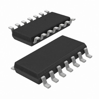
74HCT00D,653 NXP Semiconductors, 74HCT00D,653 Datasheet - Page 6

74HCT00D,653
Manufacturer Part Number
74HCT00D,653
Description
IC GATE NAND QUAD 2INPUT 14SOIC
Manufacturer
NXP Semiconductors
Series
74HCTr
Datasheet
1.74HC00D653.pdf
(16 pages)
Specifications of 74HCT00D,653
Number Of Circuits
4
Package / Case
14-SOIC (3.9mm Width), 14-SOL
Logic Type
NAND Gate
Number Of Inputs
2
Current - Output High, Low
4mA, 4mA
Voltage - Supply
4.5 V ~ 5.5 V
Operating Temperature
-40°C ~ 125°C
Mounting Type
Surface Mount
Product
NAND
Logic Family
74HCT
Propagation Delay Time
10 ns
Maximum Operating Temperature
125 C
Mounting Style
SMD/SMT
Minimum Operating Temperature
-40 C
Lead Free Status / RoHS Status
Lead free / RoHS Compliant
Lead Free Status / RoHS Status
Lead free / RoHS Compliant, Lead free / RoHS Compliant
Other names
568-1498-2
74HCT00D-T
933713370653
74HCT00D-T
933713370653
NXP Semiconductors
Table 7.
GND = 0 V; C
[1]
[2]
[3]
11. Waveforms
Table 8.
74HC_HCT00
Product data sheet
Symbol Parameter
C
74HCT00
t
t
C
Type
74HC00
74HCT00
pd
t
Fig 6.
PD
PD
t
t
C
P
f
f
C
V
N = number of inputs switching;
(C
pd
t
i
o
D
CC
PD
L
is the same as t
= input frequency in MHz;
= output frequency in MHz;
is the same as t
= output load capacitance in pF;
= C
is used to determine the dynamic power dissipation (P
= supply voltage in V;
L
V
power dissipation
capacitance
propagation delay nA, nB to nY; see
transition time
power dissipation
capacitance
Measurement points are given in
V
Input to output propagation delays
PD
OL
Dynamic characteristics
Measurement points
CC
V
L
and V
2
= 50 pF; for load circuit see
CC
f
2
o
) = sum of outputs.
OH
f
THL
PHL
i
are typical voltage output levels that occur with the output load.
N + (C
and t
and t
Input
V
0.5V
1.3 V
M
TLH
PLH
CC
Conditions
per package; V
V
per package;
V
.
CC
I
.
L
V
V
= GND to V
nA, nB input
V
CC
CC
= 4.5 V; see
nY output
CC
= 4.5 V
= 5.0 V; C
…continued
2
Table
f
GND
V
V
All information provided in this document is subject to legal disclaimers.
o
OH
OL
Figure
V
) where:
I
CC
9.
I
= GND to V
L
Figure 6
1.5 V
Figure 6
Rev. 5 — 25 November 2010
= 15 pF
7.
Output
V
0.5V
1.3 V
V
M
M
t
THL
t
PHL
CC
V
D
Y
in W):
CC
V
M
V
X
[3]
[1]
[2]
[3]
Min
t
TLH
-
-
-
-
-
t
PLH
V
0.1V
0.1V
X
25 C
CC
CC
Typ
22
12
10
22
74HC00; 74HCT00
-
001aai814
Max
-
-
-
-
-
Quad 2-input NAND gate
40 C to +125 C Unit
(85 C)
Max
24
29
V
0.9V
0.9V
-
-
-
Y
© NXP B.V. 2010. All rights reserved.
CC
CC
(125 C)
Max
29
22
-
-
-
pF
ns
ns
ns
pF
6 of 16


