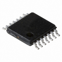
74ALVC02PW,118 NXP Semiconductors, 74ALVC02PW,118 Datasheet - Page 2

74ALVC02PW,118
Manufacturer Part Number
74ALVC02PW,118
Description
IC QUAD 2-IN NOR GATE 14TSSOP
Manufacturer
NXP Semiconductors
Series
74ALVCr
Datasheet
1.74ALVC02D118.pdf
(13 pages)
Specifications of 74ALVC02PW,118
Number Of Circuits
4
Package / Case
14-TSSOP
Logic Type
NOR Gate
Number Of Inputs
2
Current - Output High, Low
24mA, 24mA
Voltage - Supply
1.65 V ~ 3.6 V
Operating Temperature
-40°C ~ 125°C
Mounting Type
Surface Mount
Product
NOR
Logic Family
ALVC
High Level Output Current
- 24 mA
Low Level Output Current
24 mA
Propagation Delay Time
2.2 ns
Supply Voltage (max)
3.6 V
Supply Voltage (min)
1.65 V
Maximum Operating Temperature
+ 85 C
Mounting Style
SMD/SMT
Minimum Operating Temperature
- 40 C
Lead Free Status / RoHS Status
Lead free / RoHS Compliant
Lead Free Status / RoHS Status
Lead free / RoHS Compliant, Lead free / RoHS Compliant
Other names
74ALVC02PW-T
74ALVC02PW-T
935269713118
74ALVC02PW-T
935269713118
Philips Semiconductors
FEATURES
QUICK REFERENCE DATA
GND = 0 V; T
Notes
1. C
2. The condition is V
2003 Jul 14
t
C
C
PHL
SYMBOL
Wide supply voltage range from 1.65 to 3.6 V
3.6 V tolerant inputs/outputs
CMOS low power consumption
Direct interface with TTL levels (2.7 to 3.6 V)
Power-down mode
Latch-up performance exceeds 250 mA
Complies with JEDEC standard:
JESD8-7 (1.65 to 1.95 V)
JESD8-5 (2.3 to 2.7 V)
JESD8B/JESD36 (2.7 to 3.6 V).
ESD protection:
HBM EIA/JESD22-A114-A exceeds 2000 V
MM EIA/JESD22-A115-A exceeds 200 V.
I
PD
Quad 2-input NOR gate
P
f
f
C
V
N = total load switching outputs;
i
o
/t
(C
D
CC
PD
= input frequency in MHz;
L
PLH
= output frequency in MHz;
= output load capacitance in pF;
= C
L
is used to determine the dynamic power dissipation (P
= supply voltage in Volts;
PD
V
CC
amb
propagation delay nA, nB to nY
input capacitance
power dissipation capacitance per buffer
2
V
CC
= 25 C.
f
o
2
) = sum of the outputs.
I
f
= GND to V
i
N + (C
PARAMETER
L
CC
.
V
CC
2
f
o
) where:
V
V
V
V
V
2
CC
CC
CC
CC
CC
DESCRIPTION
The 74ALVC02 is a high-performance, low-power,
low-voltage, Si-gate CMOS device and superior to most
advanced CMOS compatible TTL families.
Schmitt-trigger action at all inputs makes the circuit
tolerant for slower input rise and fall times.
The 74ALVC02 provides the 2-input NOR function.
D
= 1.8 V; C
= 2.5 V; C
= 2.7 V; C
= 3.3 V; C
= 3.3 V; notes 1 and 2
in W).
CONDITIONS
L
L
L
L
= 30 pF; R
= 30 pF; R
= 50 pF; R
= 50 pF; R
L
L
L
L
= 1 k
= 500
= 500
= 500
Product specification
2.8
2.0
2.5
2.2
3.5
32
TYPICAL
74ALVC02
ns
ns
ns
ns
pF
pF
UNIT


