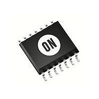
MC74LCX32DTG ON Semiconductor, MC74LCX32DTG Datasheet - Page 4

MC74LCX32DTG
Manufacturer Part Number
MC74LCX32DTG
Description
IC GATE OR QUAD 2INPUT 14-TSSOP
Manufacturer
ON Semiconductor
Series
74LVXr
Datasheet
1.MC74LCX32DR2G.pdf
(8 pages)
Specifications of MC74LCX32DTG
Logic Type
OR Gate
Number Of Inputs
2
Number Of Circuits
4
Current - Output High, Low
24mA, 24mA
Voltage - Supply
2 V ~ 3.6 V
Operating Temperature
-40°C ~ 85°C
Mounting Type
Surface Mount
Package / Case
14-TSSOP
Product
OR
Logic Family
74LCX
High Level Output Current
- 24 mA
Low Level Output Current
24 mA
Propagation Delay Time
6.2 ns
Supply Voltage (max)
3.6 V
Supply Voltage (min)
2 V
Maximum Operating Temperature
+ 85 C
Mounting Style
SMD/SMT
Minimum Operating Temperature
- 40 C
Lead Free Status / RoHS Status
Lead free / RoHS Compliant
Available stocks
Company
Part Number
Manufacturer
Quantity
Price
Company:
Part Number:
MC74LCX32DTG
Manufacturer:
ON Semiconductor
Quantity:
64
2. Skew is defined as the absolute value of the difference between the actual propagation delay for any two separate outputs of the same device.
3. Number of outputs defined as “n”. Measured with “n−1” outputs switching from HIGH−to−LOW or LOW−to−HIGH. The remaining output is
†For information on tape and reel specifications, including part orientation and tape sizes, please refer to our Tape and Reel Packaging
*This package is inherently Pb−Free.
AC CHARACTERISTICS
DYNAMIC SWITCHING CHARACTERISTICS
CAPACITIVE CHARACTERISTICS
ORDERING INFORMATION
Specifications Brochure, BRD8011/D.
MC74LCX32D
MC74LCX32DR2
MC74LCX32DR2G
MC74LCX32DT
MC74LCX32DTG
MC74LCX32DTR2
MC74LCX32DTR2G
MC74LCX32MEL
MC74LCX32MELG
Symbol
Symbol
t
t
t
t
V
V
C
C
C
Symbol
PLH
PHL
OSHL
OSLH
The specification applies to any outputs switching in the same direction, either HIGH−to−LOW (t
guaranteed by design.
measured in the LOW state.
OLP
OLV
IN
OUT
PD
Dynamic LOW Peak Voltage
(Note 3)
Dynamic LOW Valley Voltage
(Note 3)
Input Capacitance
Output Capacitance
Power Dissipation Capacitance
Propagation Delay Time
Input to Output
Output−to−Output Skew
(Note 2)
Characteristic
Device
Parameter
Parameter
t
R
= t
F
= 2.5 ns; R
Waveform
L
1
V
V
V
V
= 500 W
CC
CC
CC
CC
= 3.3 V, C
= 2.5 V, C
= 3.3 V, C
= 2.5 V, C
V
http://onsemi.com
CC
Min
1.5
1.5
MC74LCX32
C
10 MHz, V
= 3.3 V
L
L
L
L
L
= 50 pF
TSSOP−14*
TSSOP−14*
TSSOP−14*
TSSOP−14*
= 50 pF, V
= 30 pF, V
= 50 pF, V
= 30 pF, V
SOEIAJ−14
SOEIAJ−14
(Pb−Free)
(Pb−Free)
V
V
Package
SOIC−14
SOIC−14
SOIC−14
Condition
CC
CC
4
Max
= 3.3 V, V
= 3.3 V, V
5.5
5.5
1.0
1.0
0.3 V
CC
Condition
IH
IH
IH
IH
= 3.3 V, V
= 3.3 V, V
= 2.5 V, V
= 3.3 V, V
= 2.5 V, V
T
I
I
A
= 0 V or V
= 0 V or V
Min
1.5
1.5
= −40 C to +85 C
V
C
I
CC
= 0 V or V
L
Limits
IL
IL
IL
IL
= 50 pF
= 2.7 V
= 0 V
= 0 V
= 0 V
= 0 V
CC
CC
Max
6.2
6.2
OSHL
CC
Min
) or LOW−to−HIGH (t
V
CC
2500 Tape & Reel
2500 Tape & Reel
2500 Tape & Reel
2500 Tape & Reel
2000 Tape & Reel
2000 Tape & Reel
Min
1.5
1.5
T
55 Units / Rail
96 Units / Rail
96 Units / Rail
A
C
= 2.5 V
Shipping
= +25 C
L
−0.8
−0.6
Typ
0.8
0.6
Typical
= 30 pF
25
7
8
Max
6.6
6.6
0.2 V
†
Max
OSLH
); parameter
Unit
Unit
Unit
ns
ns
pF
pF
pF
V
V
V
V


