74LCX16373MTD Fairchild Semiconductor, 74LCX16373MTD Datasheet

IC LATCH TRANSP 16BIT 5V 48TSSOP

74LCX16373MTD

Manufacturer Part Number
74LCX16373MTD
Description
IC LATCH TRANSP 16BIT 5V 48TSSOP
Manufacturer
Fairchild Semiconductor
Series
74LCXr
Datasheet

Specifications of 74LCX16373MTD

Logic Type
D-Type Transparent Latch
Circuit
8:8
Output Type
Tri-State
Voltage - Supply
2 V ~ 3.6 V
Independent Circuits
2
Delay Time - Propagation
1.5ns
Current - Output High, Low
24mA, 24mA
Operating Temperature
-40°C ~ 85°C
Mounting Type
Surface Mount
Package / Case
48-TSSOP
Number Of Circuits
2
Logic Family
74LC
Polarity
Non-Inverting
Input Bias Current (max)
20 uA
High Level Output Current
- 24 mA
Low Level Output Current
24 mA
Propagation Delay Time
5.9 ns at 2.7 V, 5.4 ns at 3.3 V
Supply Voltage (max)
3.6 V
Supply Voltage (min)
2 V
Maximum Operating Temperature
+ 85 C
Minimum Operating Temperature
- 40 C
Mounting Style
SMD/SMT
Lead Free Status / RoHS Status
Lead free / RoHS Compliant

Available stocks

Company
Part Number
Manufacturer
Quantity
Price
Part Number:
74LCX16373MTD
Manufacturer:
FAIRCHILD/仙童
Quantity:
20 000
Part Number:
74LCX16373MTDX
Manufacturer:
FAIRCHILD
Quantity:
1 489
Company:
Part Number:
74LCX16373MTDX
Quantity:
478
© 2005 Fairchild Semiconductor Corporation
74LCX16373G
(Note 2)(Note 3)
74LCX16373MEA
(Note 3)
74LCX16373MTD
(Note 3)
74LCX16373
Low Voltage 16-Bit Transparent Latch
with 5V Tolerant Inputs and Outputs
General Description
The LCX16373 contains sixteen non-inverting latches with
3-STATE outputs and is intended for bus oriented applica-
tions. The device is byte controlled. The flip-flops appear
transparent to the data when the Latch Enable (LE) is
HIGH. When LE is LOW, the data that meets the setup time
is latched. Data appears on the bus when the Output
Enable (OE) is LOW. When OE is HIGH, the outputs are in
a high impedance state.
The LCX16373 is designed for low voltage (2.5V or 3.3V)
V
environment.
The LCX16373 is fabricated with an advanced CMOS tech-
nology to achieve high speed operation while maintaining
CMOS low power dissipation.
Ordering Code:
Note 2: Ordering code “G” indicates Trays.
Note 3: Devices also available in Tape and Reel. Specify by appending the suffix letter “X” to the ordering code.
Logic Symbol
Order Number
CC
applications with capability of interfacing to a 5V signal
Package Number
BGA54A
MS48A
MTD48
54-Ball Fine-Pitch Ball Grid Array (FBGA), JEDEC MO-205, 5.5mm Wide
48-Lead Small Shrink Outline Package (SSOP), JEDEC MO-118, 0.300" Wide
48-Lead Thin Shrink Small Outline Package (TSSOP), JEDEC MO-153, 6.1mm Wide
DS012002
Features
Note 1: To ensure the high-impedance state during power up or down, OE
should be tied to V
resistor is determined by the current-sourcing capability of the driver.
5V tolerant inputs and outputs
2.3V–3.6V V
5.4 ns t
Power down high impedance inputs and outputs
Supports live insertion/withdrawal (Note 1)
r
Uses patented noise/EMI reduction circuitry
Latch-up performance exceeds 500 mA
ESD performance:
Also packaged in plastic Fine-Pitch Ball Grid Array
(FBGA)
24 mA output drive (V
Human body model
Machine model
Package Description
PD
max (V
CC
CC
through a pull-up resistor: the minimum value or the
specifications provided
CC
!
200V
!
3.3V), 20
CC
2000V
3.0V)
February 1994
Revised May 2005
P
A I
CC
www.fairchildsemi.com
max

Related parts for 74LCX16373MTD

74LCX16373MTD Summary of contents

Page 1

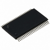
... MS48A 48-Lead Small Shrink Outline Package (SSOP), JEDEC MO-118, 0.300" Wide (Note 3) 74LCX16373MTD MTD48 48-Lead Thin Shrink Small Outline Package (TSSOP), JEDEC MO-153, 6.1mm Wide (Note 3) Note 2: Ordering code “G” indicates Trays. Note 3: Devices also available in Tape and Reel. Specify by appending the suffix letter “X” to the ordering code. ...

Page 2

Connection Diagrams Pin Assignment for SSOP and TSSOP Pin Assignment for FBGA (Top Thru View) www.fairchildsemi.com Pin Descriptions Pin Names Description OE Output Enable Input (Active LOW Latch Enable Input n I –I Inputs –O ...

Page 3

Functional Description The LCX16373 contains sixteen D-type latches with 3-STATE standard outputs. The device is byte controlled with each byte functioning identically, but independent of the other. Control pins can be shorted together to obtain full 16-bit operation. The following ...

Page 4

Absolute Maximum Ratings Symbol Parameter V Supply Voltage Input Voltage Output Voltage Input Diode Current Output Diode Current Output Source/Sink Current Supply ...

Page 5

DC Electrical Characteristics Symbol Parameter I Quiescent Supply Current Increase in I per Input CC CC Note 7: Outputs disabled or 3-STATE only. AC Electrical Characteristics Symbol Parameter t Propagation Delay PHL PLH ...

Page 6

AC LOADING and WAVEFORMS FIGURE 1. AC Test Circuit (C Test t PLH t PZL t PZH Waveform for Inverting and Non-Inverting Functions Propagation Delay. Pulse Width and t rec 3-STATE Output Low Enable and Disable Times for Logic (Input ...

Page 7

Schematic Diagram Generic for LCX Family 7 www.fairchildsemi.com ...

Page 8

Physical Dimensions inches (millimeters) unless otherwise noted 54-Ball Fine-Pitch Ball Grid Array (FBGA), JEDEC MO-205, 5.5mm Wide www.fairchildsemi.com Package Number BGA54A 8 ...

Page 9

Physical Dimensions inches (millimeters) unless otherwise noted (Continued) 48-Lead Small Shrink Outline Package (SSOP), JEDEC MO-118, 0.300" Wide Package Number MS48A 9 www.fairchildsemi.com ...

Page 10

Physical Dimensions inches (millimeters) unless otherwise noted (Continued) 48-Lead Thin Shrink Small Outline Package (TSSOP), JEDEC MO-153, 6.1mm Wide Fairchild does not assume any responsibility for use of any circuitry described, no circuit patent licenses are implied and Fairchild reserves ...

Related keywords