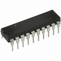
74ACTQ563PC Fairchild Semiconductor, 74ACTQ563PC Datasheet - Page 6

74ACTQ563PC
Manufacturer Part Number
74ACTQ563PC
Description
IC LATCH OCTAL 3 STATE 20-DIP
Manufacturer
Fairchild Semiconductor
Series
74ACTQr
Datasheet
1.74ACTQ563PC.pdf
(7 pages)
Specifications of 74ACTQ563PC
Logic Type
D-Type Transparent Latch
Circuit
8:8
Output Type
Tri-State
Voltage - Supply
4.5 V ~ 5.5 V
Independent Circuits
1
Delay Time - Propagation
1ns
Current - Output High, Low
24mA, 24mA
Operating Temperature
-40°C ~ 85°C
Mounting Type
Through Hole
Package / Case
20-DIP (0.300", 7.62mm)
Lead Free Status / RoHS Status
Lead free / RoHS Compliant
Other names
Q1160922
www.fairchildsemi.com
FACT Noise Characteristics
The setup of a noise characteristics measurement is critical
to the accuracy and repeatability of the tests. The following
is a brief description of the setup used to measure the
noise characteristics of FACT.
Equipment:
Procedure:
1. Verify Test Fixture Loading: Standard Load 50 pF,
2. Deskew the HFS generator so that no two channels
3. Terminate all inputs and outputs to ensure proper load-
4. Set the HFS generator to toggle all but one output at a
5. Set the HFS generator input levels at 0V LOW and 3V
Hewlett Packard Model 8180A Word Generator
PC-163A Test Fixture
Tektronics Model 7854 Oscilloscope
500 .
have greater than 150 ps skew between them. This
requires that the oscilloscope be deskewed first. It is
important to deskew the HFS generator channels
before testing. This will ensure that the outputs switch
simultaneously.
ing of the outputs and that the input levels are at the
correct voltage.
frequency of 1 MHz. Greater frequencies will increase
DUT heating and effect the results of the measure-
ment.
V
Input pulses have the following characteristics:
HIGH for ACT devices and 0V LOW and 5V HIGH for
AC devices. Verify levels with a n oscilloscope.
FIGURE 1. Quiet Output Noise Voltage Waveforms
OHV
f
1 MHz, t
and V
OLP
r
are measured with respect to ground reference.
3 ns, t
f
3 ns, skew
150 ps.
6
V
• Determine the quiet output pin that demonstrates the
• Measure V
• Verify that the GND reference recorded on the oscillo-
• Monitor one of the switching outputs using a 50 coaxial
• First increase the input LOW voltage level, V
• Next decrease the input HIGH voltage level, V
• Verify that the GND reference recorded on the oscillo-
OLP
greatest noise levels. The worst case pin will usually be
the furthest from the ground pin. Monitor the output volt-
ages using a 50
SMB type connector on the test fixture. Do not use an
active FET probe.
worst case transition for active and enable. Measure
V
case active and enable transition.
scope has not drifted to ensure the accuracy and repeat-
ability of the measurements.
V
cable plugged into a standard SMB type connector on
the test fixture. Do not use an active FET probe.
output begins to oscillate or steps out a min of 2 ns.
Oscillation is defined as noise on the output LOW level
that exceeds V
exceed V
oscillation occurs is defined as V
the output begins to oscillate or steps out a min of 2 ns.
Oscillation is defined as noise on the output LOW level
that exceeds V
exceed V
oscillation occurs is defined as V
scope has not drifted to ensure the accuracy and repeat-
ability of the measurements.
OHP
ILD
FIGURE 2. Simultaneous Switching Test Circuit
/V
OLV
and V
and V
and V
IH
IH
IHD
OLP
limits. The input LOW voltage level at which
limits. The input HIGH voltage level at which
OHV
:
OHP
and V
IL
IL
on the quiet output during the worst
limits, or on output HIGH levels that
limits, or on output HIGH levels that
/V
coaxial cable plugged into a standard
OHV
OLV
:
on the quiet output during the
ILD
IHD
.
.
IL
, until the
IH
, until


