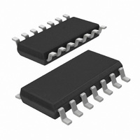
74HCT164D,653 NXP Semiconductors, 74HCT164D,653 Datasheet - Page 4

74HCT164D,653
Manufacturer Part Number
74HCT164D,653
Description
IC SHIFT REG 8BIT SI-PO 14SOIC
Manufacturer
NXP Semiconductors
Series
74HCTr
Type
Not Requiredr
Datasheet
1.74HC164D653.pdf
(20 pages)
Specifications of 74HCT164D,653
Package / Case
14-SOIC (3.9mm Width), 14-SOL
Logic Type
Shift Register
Function
Serial to Parallel
Output Type
Standard
Number Of Elements
1
Number Of Bits Per Element
8
Voltage - Supply
4.5 V ~ 6 V
Operating Temperature
-40°C ~ 125°C
Mounting Type
Surface Mount
Counting Sequence
Serial to Parallel
Number Of Circuits
1
Logic Family
HCT
Propagation Delay Time
20 ns
Supply Voltage (max)
5.5 V
Maximum Operating Temperature
+ 125 C
Minimum Operating Temperature
- 40 C
Mounting Style
SMD/SMT
Supply Voltage (min)
4.5 V
Technology
CMOS
Number Of Elements
1
Number Of Bits
8
Logical Function
Shift Register
Operating Supply Voltage (typ)
5V
Package Type
SOIC
Operating Temp Range
-40C to 125C
Operating Supply Voltage (min)
4.5V
Operating Supply Voltage (max)
5.5V
Operating Temperature Classification
Automotive
Mounting
Surface Mount
Pin Count
14
Lead Free Status / RoHS Status
Lead free / RoHS Compliant
Lead Free Status / RoHS Status
Lead free / RoHS Compliant, Lead free / RoHS Compliant
Other names
74HCT164D-T
74HCT164D-T
933714080653
74HCT164D-T
933714080653
NXP Semiconductors
Table 2.
6. Functional description
Table 3.
[1]
7. Limiting values
Table 4.
In accordance with the Absolute Maximum Rating System (IEC 60134). Voltages are referenced to GND (ground = 0 V).
74HC_HCT164
Product data sheet
Symbol
DSA
DSB
Q0 to Q7
GND
CP
MR
V
Operating
modes
Reset (clear)
Shift
Symbol
V
I
I
I
I
I
T
IK
OK
O
CC
GND
stg
CC
CC
H = HIGH voltage level
h = HIGH voltage level one set-up time prior to the LOW-to-HIGH clock transition
L = LOW voltage level
I = LOW voltage level one set-up time prior to the LOW-to-HIGH clock transition
q = lower case letters indicate the state of the referenced input one set-up time prior to the LOW-to-HIGH clock transition
= LOW-to-HIGH clock transition
Pin description
Function table
Limiting values
Parameter
supply voltage
input clamping current
output clamping current
output current
supply current
ground current
storage temperature
5.2 Pin description
Input
MR
L
H
H
H
H
3, 4, 5, 6, 10, 11, 12, 13
7
[1]
Pin
1
2
8
9
14
CP
X
All information provided in this document is subject to legal disclaimers.
Rev. 5 — 25 November 2010
Conditions
V
V
0.5 V < V
I
O
< 0.5 V or V
DSA
X
l
l
h
h
< 0.5 V or V
O
< V
I
CC
O
> V
> V
+ 0.5 V
CC
DSB
X
l
h
l
h
Description
data input
data input
output
ground (0 V)
clock input (LOW-to-HIGH, edge-triggered)
master reset input (active LOW)
positive supply voltage
CC
+ 0.5 V
+ 0.5 V
74HC164; 74HCT164
8-bit serial-in, parallel-out shift register
Output
Q0
L
L
L
L
H
[1]
[1]
Min
0.5
-
-
-
-
50
65
© NXP B.V. 2010. All rights reserved.
Q1 to Q7
L to L
q0 to q6
q0 to q6
q0 to q6
q0 to q6
Max
+7
20
20
25
50
-
+150
Unit
V
mA
mA
mA
mA
mA
C
4 of 20


