SY89841UMG TR Micrel Inc, SY89841UMG TR Datasheet - Page 4
SY89841UMG TR
Manufacturer Part Number
SY89841UMG TR
Description
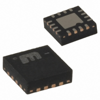
IC MUX 2:1 LVDS RPE 16-MLF
Manufacturer
Micrel Inc
Series
SY89r
Type
Multiplexerr
Datasheet
1.SY89841UMG.pdf
(15 pages)
Specifications of SY89841UMG TR
Circuit
1 x 2:1
Independent Circuits
1
Voltage Supply Source
Single Supply
Voltage - Supply
3 V ~ 3.6 V
Operating Temperature
-40°C ~ 85°C
Mounting Type
Surface Mount
Package / Case
16-MLF®, QFN
Number Of Clock Inputs
2
Mode Of Operation
Differential
Output Logic Level
LVDS
Operating Supply Voltage (min)
2.375V
Operating Supply Voltage (typ)
2.5V
Operating Supply Voltage (max)
2.625V
Package Type
MLF
Operating Temp Range
-40C to 85C
Operating Temperature Classification
Industrial
Signal Type
CML/LVDS/PECL
Mounting
Surface Mount
Pin Count
16
Lead Free Status / RoHS Status
Lead free / RoHS Compliant
Current - Output High, Low
-
Lead Free Status / Rohs Status
Compliant
Other names
SY89841UMGTR
SY89841UMGTR
SY89841UMGTR


Micrel, Inc.
Pin Description
Truth Table
February 2005
Pin Number
5, 8, 12
16, 13
2, 14
3, 15
4, 1,
6, 7
10
11
9
Exposed Pad
VREF-AC0
VREF-AC1
Pin Name
IN0, /IN0,
VT0, VT1
IN1, /IN1
Q, /Q
VCC
GND
CAP
SEL
IN0
X
X
0
1
/IN0
X
X
1
0
Pin Function
Differential Inputs: These input pairs are the differential signal inputs to the
device. These inputs accept AC- or DC-coupled signals as small as 100mV.
Each pin of a pair internally terminates to a VT pin through 50 . Please refer to
the “Input Interface Applications” section for more details.
Reference Voltage: This output biases to V
inputs IN and /IN. Connect V
with 0.01µF low ESR capacitor to V
Due to the limited drive capability, the VREF-AC pin is only intended to drive its
respective VT pin. See the “Input Interface Applications” section for more details.
Input Termination Center-Tap: Each side of the differential input pair terminates
to a VT pin. The VT0 and VT1 pins provide a center-tap to a termination network
for maximum interface flexibility. See the “Input Interface Applications” section
for more details.
Positive Power Supply: Bypass with 0.1µF//0.01µF low ESR capacitors as close
to the VCC pins as possible.
Differential Outputs: This LVDS differential output is a logic function of the IN0,
IN1, and SEL inputs. Please refer to the truth table below for details.
This single-ended TTL/CMOS-compatible input selects the inputs to the
multiplexer. Note that this input is internally connected to a 25k pull-up resistor
and will default to logic HIGH state if left open.
Ground: Ground and exposed pad must be connected to the same ground
plane.
Power-On Reset (POR) Initialization capacitor. When using the multiplexer with
RPE capability, this pin is tied to a capacitor to V
internal RPE logic starts up in a known state. See “Power-On Reset (POR)
Description” section for more details regarding capacitor selection. If this pin is
tied directly to V
function as a normal multiplexer. The CAP pin should never be left open.
Inputs
IN1
X
X
0
1
CC
/IN1
, the RPE function will be disabled and the multiplexer will
X
X
4
1
0
SEL
0
0
1
1
REF-AC
directly to the corresponding VT pin. Bypass
CC
. Maximum sink/source current is ±1.5mA.
Q
0
1
0
1
Outputs
CC
hbwhelp@micrel.com
–1.2V. It is used for AC-coupling
/Q
1
0
1
0
CC
. The purpose is to ensure the
or (408) 955-1690
M9999-021405
SY89841U
Related parts for SY89841UMG TR
Image
Part Number
Description
Manufacturer
Datasheet
Request
R

Part Number:
Description:
Manufacturer:
Micrel Inc
Datasheet:
Part Number:
Description:
Manufacturer:
Micrel Inc
Datasheet:
Part Number:
Description:
Manufacturer:
Micrel Inc
Datasheet:
Part Number:
Description:
Manufacturer:
Micrel Inc
Datasheet:
Part Number:
Description:
Manufacturer:
Micrel Inc
Datasheet:
Part Number:
Description:
Manufacturer:
Micrel Inc
Datasheet:
Part Number:
Description:
Manufacturer:
Micrel Inc
Datasheet:
Part Number:
Description:
Manufacturer:
Micrel Inc
Datasheet:
Part Number:
Description:
Manufacturer:
Micrel Inc
Datasheet:
Part Number:
Description:
Manufacturer:
Micrel Inc
Datasheet:
Part Number:
Description:
Manufacturer:
Micrel Inc
Datasheet:
Part Number:
Description:
Manufacturer:
Micrel Inc
Datasheet:
Part Number:
Description:
Manufacturer:
Micrel Inc
Datasheet:
Part Number:
Description:
Manufacturer:
Micrel Inc
Datasheet: