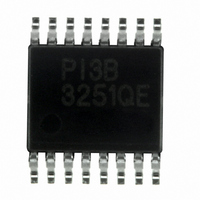
PI3B3251QE Pericom Semiconductor, PI3B3251QE Datasheet - Page 2

PI3B3251QE
Manufacturer Part Number
PI3B3251QE
Description
IC 8-1 MUX/DEMUX BUS SW 16-QSOP
Manufacturer
Pericom Semiconductor
Type
Multiplexer/Demultiplexerr
Datasheet
1.PI3B3251QE.pdf
(5 pages)
Specifications of PI3B3251QE
Circuit
1 x 8:1
Independent Circuits
1
Voltage Supply Source
Single Supply
Voltage - Supply
3.3V
Operating Temperature
-40°C ~ 85°C
Mounting Type
Surface Mount
Package / Case
16-QSOP
Lead Free Status / RoHS Status
Lead free / RoHS Compliant
Current - Output High, Low
-
Available stocks
Company
Part Number
Manufacturer
Quantity
Price
Part Number:
PI3B3251QEX
Manufacturer:
PERICOM
Quantity:
20 000
Maximum Ratings
(Above which the useful life may be impaired. For user guidelines, not tested.)
Notes:
1.
2.
3.
Capacitance
Note:
1.
DC Electrical Characteristics
Parameters
Storage Temperature ..................................................................... –65°C to +150°C
Ambient Temperature with Power Applied .................................... –40°C to +85°C
Supply Voltage to Ground Potential ................................................–0.5V to +4.6V
DC Input Voltage .............................................................................–0.5V to +4.6V
DC Output Current ........................................................................................ 120mA
Power Dissipation ............................................................................................ 0.5W
For Max. or Min. conditions, use appropriate value specifi ed under Electrical Characteristics for the applicable device type.
Typical values are at V
Measured by the voltage drop between I and Y pin at indicated current through the switch. On-Resistance is determined by the lower of the
voltages on the two (I,Y) pins.
This parameter is determined by device characterization but is not production tested.
Parameters
I
R
V
V
V
OZH
I
I
IH
ON
IL
IH
IK
IL
C
09-0037
C
C
Y(OFF)
I(OFF)
C
I(ON)
IN
Input HIGH Voltage
Input LOW Voltage
Input HIGH Current
Input LOW Current
High Impedance Output Current
Clamp Diode Voltage
Switch On-Resistance
(T
(1)
A
= 25°C, f = 1 MHz)
CC
Input Capacitance
I
Y Capacitance, Switch Off
I
0
0
De scrip tion
- I
- I
= 3.3V, T
7
7
Capacitance, Switch Off
Capacitance, Switch On
A
(3)
= 25°C ambient and maximum loading.
(Over the Operating Range, T
De scrip tion
Guaranteed Logic HIGH Level
Guaranteed Logic LOW Level
V
V
0 ≤ I
V
V
I
V
I
ON
ON
CC
CC
CC
CC
CC
= 48mA or 64mA
= 15mA
N
= Max., V
= Max., V
= Min., I
= Min., V
= Min., V
, Y ≤ V
Test Conditions
2
CC
IN
A
IN
IN
IN
IN
= –40°C to +85°C, V
= –18mA
= 0.0V,
= 2.4V,
= V
= GND
CC
(1)
Test Conditions
V
3.3V, 8:1 Mux/DeMux NanoSwitch
IN
Note:
Stresses greater than those listed under MAX I MUM
RATINGS may cause per ma nent dam age to the
device. This is a stress rating only and func tion al
op er a tion of the device at these or any other condi-
tions above those indicated in the operational sec-
tions of this specifi cation is not implied. Ex po sure
to absolute maximum rating conditions for ex tend ed
periods may affect reliability.
= 0V
CC
Min.
–0.5
2.0
=3.3V ±10%)
Typ
10
5
(2)
Typ.
64.0
72.0
3.0
8.0
PS8150G
Max.
–1.2
0.8
±1
±1
±1
17
8
PI3B3251
Units
pF
Units
μA
V
V
Ω
03/02/09
™


