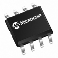
24LC024H-I/MS Microchip Technology, 24LC024H-I/MS Datasheet - Page 16

24LC024H-I/MS
Manufacturer Part Number
24LC024H-I/MS
Description
IC EEPROM 2KBIT 400KHZ 8MSOP
Manufacturer
Microchip Technology
Specifications of 24LC024H-I/MS
Memory Size
2K (256 x 8)
Package / Case
8-MSOP, Micro8™, 8-uMAX, 8-uSOP,
Format - Memory
EEPROMs - Serial
Memory Type
EEPROM
Speed
400kHz
Interface
I²C, 2-Wire Serial
Voltage - Supply
2.5 V ~ 5.5 V
Operating Temperature
-40°C ~ 85°C
Organization
256 K x 8
Interface Type
I2C
Maximum Clock Frequency
1 MHz
Access Time
400 ns
Supply Voltage (max)
5.5 V
Supply Voltage (min)
2.5 V
Maximum Operating Current
3 mA
Maximum Operating Temperature
+ 85 C
Mounting Style
SMD/SMT
Minimum Operating Temperature
- 40 C
Operating Supply Voltage
3.3 V, 5 V
Lead Free Status / RoHS Status
Lead free / RoHS Compliant
Lead Free Status / RoHS Status
Lead free / RoHS Compliant, Lead free / RoHS Compliant
24AAXX/24LCXX/24FCXX
6.0
6.1
A byte write operation begins with a Start condition
from the master followed by the four-bit control code
(see Figure 6-1 and Figure 6-2). The next 3 bits are
either the Block Address bits (for devices without
address pins) or the Chip Select bits (for devices with
address pins). Then the master transmitter clocks the
R/W bit (which is a logic low) onto the bus. The slave
then generates an Acknowledge bit during the ninth
clock cycle.
The next byte transmitted by the master is the address
byte (for 128-bit to 16 Kbit devices) or the high-order
address byte (for 32-1024 Kbit devices). For 32 through
1024 Kbit devices, the high-order address byte is
followed by the low-order address byte. In either case,
each address byte is acknowledged by the 24XX and
the address bits are latched into the internal address
counter of the 24XX.
FIGURE 6-1:
FIGURE 6-2:
DS21930C-page 16
SDA Line
Bus Activity
Master
Bus Activity
Bus Activity
Master
SDA Line
Bus Activity
WRITE OPERATIONS
Byte Write
S
S
T
A
R
T
S
S
T
A
R
T
BYTE WRITE: 128-BIT TO 16 KBIT DEVICES
BYTE WRITE: 32 TO 1024 KBIT DEVICES
Control
Byte
Control
Byte
A
C
K
Address Byte
High Order
A
C
K
A
C
K
Address
Address Byte
Low Order
Byte
For the 24XX00 devices, only the lower four address
bits are used by the device. The upper four bits are
“don’t cares.”
After receiving the ACK from the 24XX acknowledging
the final address byte, the master device transmits the
data word to be written into the addressed memory
location. The 24XX acknowledges again and the
master generates a Stop condition, which initiates the
internal write cycle.
If an attempt is made to write to an array with the WP
pin held high, the device will acknowledge the
command, but no write cycle will occur, no data will be
written, and the device will immediately accept a new
command. After a byte Write command, the internal
address counter will increment to the next address
location. During a write cycle, the 24XX will not
acknowledge commands.
A
C
K
A
C
K
Data
Byte
© 2007 Microchip Technology Inc.
Data
Byte
A
C
K
O
S
T
P
P
A
C
K
P
S
T
O
P


