CY7C1021BNV33L-15ZXI Cypress Semiconductor Corp, CY7C1021BNV33L-15ZXI Datasheet
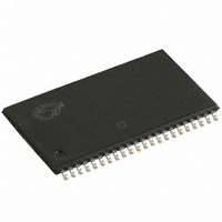
IC SRAM 1MBIT 15NS 44TSOP

CY7C1021BNV33L-15ZXI

Manufacturer Part Number
CY7C1021BNV33L-15ZXI
Description
IC SRAM 1MBIT 15NS 44TSOP
Manufacturer
Cypress Semiconductor Corp
Type
Asynchronousr

Specifications of CY7C1021BNV33L-15ZXI

Memory Size
1M (64K x 16)
Package / Case
44-TSOP II
Format - Memory
RAM
Memory Type
SRAM - Asynchronous
Speed
15ns
Interface
Parallel
Voltage - Supply
3 V ~ 3.6 V
Operating Temperature
-40°C ~ 85°C
Access Time
15 ns
Supply Voltage (max)
3.63 V
Supply Voltage (min)
2.97 V
Maximum Operating Current
160 mA
Maximum Operating Temperature
+ 85 C
Minimum Operating Temperature
- 40 C
Mounting Style
SMD/SMT
Number Of Ports
1
Operating Supply Voltage
3.3 V
Density
1Mb
Access Time (max)
15ns
Sync/async
Asynchronous
Architecture
Not Required
Clock Freq (max)
Not RequiredMHz
Operating Supply Voltage (typ)
3.3V
Address Bus
16b
Package Type
TSOP-II
Operating Temp Range
-40C to 85C
Supply Current
160mA
Operating Supply Voltage (min)
2.97V
Operating Supply Voltage (max)
3.63V
Operating Temperature Classification
Industrial
Mounting
Surface Mount
Pin Count
44
Word Size
16b
Number Of Words
64K
Lead Free Status / RoHS Status
Lead free / RoHS Compliant
Lead Free Status / RoHS Status
Lead free / RoHS Compliant, Lead free / RoHS Compliant

Available stocks

Company
Part Number
Manufacturer
Quantity
Price
Part Number:
CY7C1021BNV33L-15ZXI
Manufacturer:
CYPRESS
Quantity:
1 000
Cypress Semiconductor Corporation
Document #: 001-06433 Rev. *B
Features
Note:
1. For guidelines on SRAM system design, please refer to the ‘System Design Guidelines’ Cypress application note, available on the internet at www.cypress.com
Logic Block Diagram
• 3.3V operation (3.0V–3.6V)
• High speed
• CMOS for optimum speed/power
• Low Active Power (L version)
• Low CMOS Standby Power (L version)
• Automatic power-down when deselected
• Independent control of upper and lower bits
• Available in 44-pin TSOP II and 400-mil SOJ
• Available in a 48-Ball Mini BGA package
— t
— 576 mW (max.)
— 1.80 mW (max.)
A
A
A
A
A
A
A
A
4
3
2
1
0
7
6
5
AA
= 10, 12, 15 ns
DATA IN DRIVERS
COLUMN DECODER
512 X 2048
RAM Array
64K x 16
198 Champion Court
Functional Description
The CY7C1021BNV is a high-performance CMOS static RAM
organized as 65,536 words by 16 bits. This device has an
automatic power-down feature that significantly reduces
power consumption when deselected.
Writing to the device is accomplished by taking Chip Enable
(CE) and Write Enable (WE) inputs LOW. If Byte Low Enable
(BLE) is LOW, then data from I/O pins (I/O
written into the location specified on the address pins (A
through A
from I/O pins (I/O
specified on the address pins (A
Reading from the device is accomplished by taking Chip
Enable (CE) and Output Enable (OE) LOW while forcing the
Write Enable (WE) HIGH. If Byte Low Enable (BLE) is LOW,
then data from the memory location specified by the address
pins will appear on I/O
LOW, then data from memory will appear on I/O
the truth table at the back of this data sheet for a complete
description of read and write modes.
The input/output pins (I/O
high-impedance state when the device is deselected
(CE HIGH), the outputs are disabled (OE HIGH), the BHE and
BLE are disabled (BHE, BLE HIGH), or during a write
operation (CE LOW, and WE LOW).
The CY7C1021BNV is available in 400-mil-wide SOJ,
standard 44-pin TSOP Type II, and 48-ball mini BGA
packages.
I/O
I/O
15
San Jose
1
9
BHE
WE
CE
OE
BLE
). If Byte High Enable (BHE) is LOW, then data
–I/O
–I/O
8
16
9
through I/O
,
64K x 16 Static RAM
CA 95134-1709
1
to I/O
I/O 1
I/O 2
I/O 3
I/O 4
V
I/O 5
I/O 6
I/O 7
I/O 8
V
Pin Configurations
WE
A 15
A 14
A 13
A 12
NC
CE
A
A 3
A 2
A 1
A 0
CC
SS
1
4
through I/O
SOJ / TSOP II
[1]
8
1
2
3
4
5
6
7
8
9
10
11
12
13
14
15
16
17
18
19
20
21
22
. If Byte High Enable (BHE) is
16
Top View
0
Revised December 14, 2010
CY7C1021BNV33
) is written into the location
through A
44
43
42
41
40
39
38
37
36
35
34
33
32
31
30
29
28
27
26
25
24
23
16
A 5
A 6
A 7
OE
BHE
BLE
I/O 16
I/O 15
I/O 14
I/O 13
V
V
I/O 12
I/O 11
I/O 10
I/O 9
NC
A 8
A 9
A 10
A 11
NC
) are placed in a
1
15
SS
CC
through I/O
).
9
408-943-2600
to I/O
16 .
8
See
), is
0
[+] Feedback

Related parts for CY7C1021BNV33L-15ZXI

CY7C1021BNV33L-15ZXI Summary of contents

Page 1

... COLUMN DECODER Note: 1. For guidelines on SRAM system design, please refer to the ‘System Design Guidelines’ Cypress application note, available on the internet at www.cypress.com Cypress Semiconductor Corporation Document #: 001-06433 Rev. *B Functional Description The CY7C1021BNV is a high-performance CMOS static RAM organized as 65,536 words by 16 bits. This device has an automatic power-down feature that significantly reduces power consumption when deselected ...

Page 2

Selection Guide Maximum Access Time (ns) Maximum Operating Current (mA) Maximum CMOS Standby Current (mA) Pin Configurations Document #: 001-06433 Rev. *B -10 10 Commercial 160 Industrial 180 Commercial/Industrial 5 L 0.5 Mini BGA (Top View ...

Page 3

Maximum Ratings (Above which the useful life may be impaired. For user guide- lines, not tested.) Storage Temperature .............................. – +150 C Ambient Temperature with Power Applied.......................................... – +125 C Supply Voltage Relative ...

Page 4

... At any given temperature and voltage condition The internal write time of the memory is defined by the overlap of CE LOW, WE LOW and BHE / BLE LOW. CE, WE and BHE / BLE must be LOW to initiate a write, and the transition of these signals can terminate the write. The input data set-up and hold timing should be referenced to the leading edge of the signal that terminates the write ...

Page 5

Data Retention Waveform Switching Waveforms [10, 11] Read Cycle No. 1 ADDRESS DATA OUT PREVIOUS DATA VALID [11, 12] Read Cycle No. 2 (OE Controlled) ADDRESS CE t ACE OE t BHE, BLE t LZOE t DBE ...

Page 6

Switching Waveforms (continued) [13, 14] Write Cycle No. 1 (CE Controlled) ADDRESS BHE, BLE DATA I/O Write Cycle No. 2 (BLE or BHE Controlled) ADDRESS t SA BHE, BLE WE CE DATA I/O Notes: 13. Data ...

Page 7

Switching Waveforms (continued) Write Cycle No. 2 (WE Controlled, OE LOW) ADDRESS BHE, BLE DATA I/O Truth Table BLE BHE I High ...

Page 8

... Cypress maintains a worldwide network of offices, solution centers, manufacturer's representatives and distributors. To find the office closest to you, visit us at http://www.cypress.com/go/datasheet/offices. Speed (ns) Ordering Code 15 CY7C1021BNV33L-15BAI CY7C1021BNV33L-15VXI CY7C1021BNV33L-15ZXI Ordering Code Definitions V33 L Please contact local sales representative regarding availability of these parts. ...

Page 9

Package Diagrams 48-ball FBGA ( 1.2 mm) (51-85096) TOP VIEW PIN 1 CORNER (LASER MARK 7.00±0.10 SIDE VIEW SEATING ...

Page 10

Package Diagrams (continued) All product and company names mentioned in this document may be the trademarks of their respective holders. Document #: 001-06433 Rev. *B 44-Pin TSOP Type II (51-85087) 51-85087 *C CY7C1021BNV33 51-85087-*A Page [+] Feedback ...

Page 11

... Document #: 001-06433 Rev. *B © Cypress Semiconductor Corporation, 2006-2010. The information contained herein is subject to change without notice. Cypress Semiconductor Corporation assumes no responsibility for the use of any circuitry other than circuitry embodied in a Cypress product. Nor does it convey or imply any license under patent or other rights. Cypress products are not warranted nor intended to be used for medical, life support, life saving, critical control or safety applications, unless pursuant to an express written agreement with Cypress ...

Related keywords