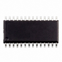
M48Z35Y-70MH1F STMicroelectronics, M48Z35Y-70MH1F Datasheet - Page 10

M48Z35Y-70MH1F
Manufacturer Part Number
M48Z35Y-70MH1F
Description
IC NVSRAM 256KBIT 70NS 28SOIC
Manufacturer
STMicroelectronics
Datasheet
1.M48Z35Y-70MH1F.pdf
(24 pages)
Specifications of M48Z35Y-70MH1F
Format - Memory
RAM
Memory Type
NVSRAM (Non-Volatile SRAM)
Memory Size
256K (32K x 8)
Speed
70ns
Interface
Parallel
Voltage - Supply
4.5 V ~ 5.5 V
Operating Temperature
0°C ~ 70°C
Package / Case
28-SOIC, 28-SOH (8.48mm Width)
Lead Free Status / RoHS Status
Lead free / RoHS Compliant
Other names
497-4728-2
Available stocks
Company
Part Number
Manufacturer
Quantity
Price
Operating modes
2.2
Figure 6.
Figure 7.
10/24
A0-A14
E
W
DQ0-DQ7
A0-A14
E
W
DQ0-DQ7
WRITE mode
The M48Z35/Y is in the WRITE mode whenever W and E are low. The start of a WRITE is
referenced from the latter occurring falling edge of W or E. A WRITE is terminated by the
earlier rising edge of W or E. The addresses must be held valid throughout the cycle. E or W
must return high for a minimum of t
to the initiation of another READ or WRITE cycle. Data-in must be valid t
end of WRITE and remain valid for t
cycles to avoid bus contention; although, if the output bus has been activated by a low on E
and G, a low on W will disable the outputs t
WRITE enable controlled, WRITE AC waveforms
Chip enable controlled, WRITE AC waveforms
tAVEL
tAVEL
tAVWL
tAVWL
tWLQZ
Doc ID 2608 Rev 9
tAVWH
tAVEH
EHAX
tWLWH
VALID
tAVAV
VALID
tAVAV
WHDX
tELEH
from chip enable or t
afterward. G should be kept high during WRITE
WLQZ
tDVEH
tDVWH
DATA INPUT
after W falls.
DATA INPUT
tWHDX
WHAX
tEHDX
tWHQX
from WRITE enable prior
tEHAX
tWHAX
M48Z35, M48Z35Y
DVWH
prior to the
AI00926
AI00927


