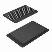
CY7C1370D-200BGXC Cypress Semiconductor Corp, CY7C1370D-200BGXC Datasheet - Page 16

CY7C1370D-200BGXC
Manufacturer Part Number
CY7C1370D-200BGXC
Description
IC SRAM 18MBIT 200MHZ 119BGA
Manufacturer
Cypress Semiconductor Corp
Type
Synchronousr
Specifications of CY7C1370D-200BGXC
Memory Size
18M (512K x 36)
Package / Case
119-BGA
Format - Memory
RAM
Memory Type
SRAM - Synchronous
Speed
200MHz
Interface
Parallel
Voltage - Supply
3.135 V ~ 3.6 V
Operating Temperature
0°C ~ 70°C
Access Time
3 ns
Maximum Clock Frequency
200 MHz
Supply Voltage (max)
3.6 V
Supply Voltage (min)
3.135 V
Maximum Operating Current
300 mA
Maximum Operating Temperature
+ 70 C
Minimum Operating Temperature
0 C
Mounting Style
SMD/SMT
Number Of Ports
4
Operating Supply Voltage
3.3 V
Lead Free Status / RoHS Status
Lead free / RoHS Compliant
Lead Free Status / RoHS Status
Lead free / RoHS Compliant, Lead free / RoHS Compliant
Available stocks
Company
Part Number
Manufacturer
Quantity
Price
Company:
Part Number:
CY7C1370D-200BGXC
Manufacturer:
Cypress Semiconductor Corp
Quantity:
10 000
Identification Codes
119-ball BGA Boundary Scan Order
Document Number: 38-05558 Rev. *H
EXTEST
IDCODE
SAMPLE Z
RESERVED
SAMPLE/PRELOAD
RESERVED
RESERVED
BYPASS
Notes
12. Balls which are NC (No Connect) are pre-set LOW.
13. Bit# 85 is pre-set HIGH.
Bit #
10
11
12
13
14
15
16
17
18
19
20
21
22
1
2
3
4
5
6
7
8
9
Instruction
Ball ID
M6
G7
H4
R5
R6
U6
R7
P6
N7
K6
P7
N6
K7
H6
T4
T5
T6
L5
T7
L7
L6
J5
Code
000
001
010
011
100
101
110
111
Bit #
Captures I/O ring contents. Places the boundary scan register between TDI and TDO.
Forces all SRAM outputs to high Z state.
Loads the ID register with the vendor ID code and places the register between TDI and
TDO. This operation does not affect SRAM operations.
Captures I/O ring contents. Places the boundary scan register between TDI and TDO.
Forces all SRAM output drivers to a high Z state.
Do Not Use: This instruction is reserved for future use.
Captures I/O ring contents. Places the boundary scan register between TDI and TDO.
Does not affect SRAM operation.
Do Not Use: This instruction is reserved for future use.
Do Not Use: This instruction is reserved for future use.
Places the bypass register between TDI and TDO. This operation does not affect SRAM
operations.
23
24
25
26
27
28
29
30
31
32
33
34
35
36
37
38
39
40
41
42
43
44
Ball ID
M4
E7
D7
H7
G6
E6
D6
C7
B7
C6
A6
C5
B5
G5
B6
D4
B4
A5
K4
E4
[12, 13]
F6
F4
Bit #
45
46
47
48
49
50
51
52
53
54
55
56
57
58
59
60
61
62
63
64
65
66
Description
Ball ID
G4
G3
G1
G2
A4
C3
B2
B3
A3
C2
A2
B1
C1
D2
E1
F2
H2
D1
E2
H1
2K
J3
Bit #
67
68
69
70
71
72
73
74
75
76
77
78
79
80
81
82
83
84
85
CY7C1370DV25
CY7C1372DV25
Internal
Ball ID
Page 16 of 29
M2
N1
N2
R3
R1
R2
N4
P1
K1
P2
T1
T2
T3
P4
L1
L2
L3
L4
[+] Feedback


