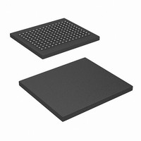
CY7C1512V18-250BZC Cypress Semiconductor Corp, CY7C1512V18-250BZC Datasheet - Page 28

CY7C1512V18-250BZC
Manufacturer Part Number
CY7C1512V18-250BZC
Description
IC SRAM 72MBIT 250MHZ 165TFBGA
Manufacturer
Cypress Semiconductor Corp
Datasheet
1.CY7C1512V18-167BZXC.pdf
(29 pages)
Specifications of CY7C1512V18-250BZC
Format - Memory
RAM
Memory Type
SRAM - Synchronous, QDR II
Memory Size
72M (4M x 18)
Speed
250MHz
Interface
Parallel
Voltage - Supply
1.7 V ~ 1.9 V
Operating Temperature
0°C ~ 70°C
Package / Case
165-TFBGA
Lead Free Status / RoHS Status
Contains lead / RoHS non-compliant
Available stocks
Company
Part Number
Manufacturer
Quantity
Price
Company:
Part Number:
CY7C1512V18-250BZC
Manufacturer:
Cypress Semiconductor Corp
Quantity:
10 000
Document History Page
Document #: 38-05489 Rev. *F
Document Title: CY7C1510V18/CY7C1525V18/CY7C1512V18/CY7C1514V18, 72-Mbit QDR™-II SRAM 2-Word
Burst Architecture
Document Number: 38-05489
REV.
*A
*B
*C
**
ECN NO.
201260
257089
319496
403231
See ECN
See ECN
See ECN
See ECN
ISSUE
DATE
ORIG. OF
CHANGE
NXR
SYT
NJY
NJY
DESCRIPTION OF CHANGE
New Data Sheet
Removed foot note 13 on page 12
Modified JTAG ID register definition table on page 21
Changed Max. value of t
Max. value of t
Changed Max. value of t
Max. value of t
Included thermal values
Modified capacitance values table: included capacitance values for x8, x18 and x36
options
Removed CY7C1525V18 from the title
Included 300-MHz Speed bin
Added footnote #1 and accordingly edited the V
Definitions table.
Added Industrial Temperature Grade
Replaced TBDs for I
grades
Changed the C
Removed the capacitance value column for the x9 option from Capacitance Table
Changed typo of bit # 47 to bit # 108 under the EXTEST OUTPUT BUS TRI-STATE on
Page 18
Added lead-free product information
Updated the Ordering Information by Shading and Unshading MPNs as per availability
Converted from Preliminary to Final
Added CY7C1525V18 to the title
Removed 300-MHz Speed bin
Changed address of Cypress Semiconductor Corporation on Page# 1 from “3901 North
First Street” to “198 Champion Court”
Changed C/C Pin Description in the features section and Pin Description
Added power-up sequence details and waveforms
Added foot notes # 14, 15, 16 on page# 19
Replaced Three-state with Tri-state
Changed the description of I
page# 20, Modified the I
Modified test condition in Footnote # 21 on page# 20 from V
Replaced Package Name column with Package Diagram in the Ordering
Information table, Updated the Ordering Information .
cyc
KHCH
IN
from 5 pF to 5.5 pF and C
@ 200 MHz from 6.3 ns to 7.9 ns.
DD
@ 167 MHz from 2.8 ns to 2.7 ns
and I
DD
cyc
KHCH
and I
@ 250 MHz from 5.25 ns to 6.3 ns and
SB1
X
from Input Load Current to Input Leakage Current on
@ 200 MHz from 2.3 ns to 2.2 ns and
for 300 MHz, 250 MHz, 200 MHz and 167 MHz speed
SB
current values
CY7C1510V18, CY7C1525V18
CY7C1512V18, CY7C1514V18
O
from 7 pF to 8 pF in the Capacitance Table
SS
/144M And V
DDQ
SS
< V
/288M on the Pin
DD
to V
Page 28 of 29
DDQ
< V
DD
[+] Feedback


