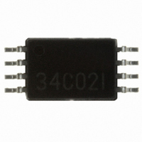
CAT34C02YI-G ON Semiconductor, CAT34C02YI-G Datasheet

CAT34C02YI-G
Specifications of CAT34C02YI-G
Available stocks
Related parts for CAT34C02YI-G
CAT34C02YI-G Summary of contents
Page 1
... CAT34C02 Figure 1. Functional Symbol *For additional information on our Pb−Free strategy and soldering details, please download the ON Semiconductor Soldering and Mounting Techniques Reference Manual, SOLDERRM/D. © Semiconductor Components Industries, LLC, 2011 March, 2011 − Rev protocol Bus Inputs Pin Name A 0 SDA See detailed ordering and shipping information in the package dimensions section on page 14 of this data sheet ...
Page 2
Table 1. ABSOLUTE MAXIMUM RATINGS Operating Temperature Storage Temperature Voltage on Any Pin with Respect to Ground (Note 1) Voltage on Pin A with Respect to Ground 0 Stresses exceeding Maximum Ratings may damage the device. Maximum Ratings are stress ...
Page 3
Table 5. A.C. CHARACTERISTICS Symbol F Clock Frequency SCL t START Condition Hold Time HD:STA t Low Period of SCL Clock LOW t High Period of SCL Clock HIGH t START Condition Setup Time SU:STA t Data Hold Time HD:DAT ...
Page 4
Power−On Reset (POR) The CAT34C02 incorporates Power−On Reset (POR) circuitry which protects the internal logic against powering up in the wrong state. The CAT34C02 will power up into Standby mode after V exceeds the POR trigger level and will power ...
Page 5
... Read’ command (see READ OPERATIONS). The CAT34C02 will not acknowledge the Slave address, as long as internal Write is in progress. Delivery State The CAT34C02 is shipped ‘unprotected’, i.e. neither SWP flag is set. The entire 2 kb memory is erased, i.e. all bytes are FFh. http://onsemi.com 5 A ...
Page 6
BUS ACTIVITY: R MASTER T SDA LINE S SCL 8th Bit SDA Byte BUS ACTIVITY: SLAVE R MASTER ADDRESS T SDA LINE NOTE: IN THIS EXAMPLE n = XXXX ...
Page 7
... CAT34C02, then the device will continue th clock cycle, transmitting as long as each data byte is acknowledged by the Master (Figure 12). If the end of memory is reached during sequential Read, then the address counter will ‘wrap−around’ to the beginning of memory, etc. Sequential Read works with either ‘Immediate Address Read’ or ‘ ...
Page 8
... For Write commands a dummy byte address and dummy data byte must be provided (Figure 14). In contrast to a regular memory Read, a SWP Read does not return Data. Instead the CAT34C02 will respond with NoACK if the flag Table 8. RSWP D.C. OPERATING CONDITIONS ...
Page 9
Table 9. SWP COMMANDS Control Pin Levels (Note 12) Action PSWP GND Set PSWP ...
Page 10
E1 e TOP VIEW SIDE VIEW Notes: (1) All dimensions are in millimeters. Angles in degrees. (2) Complies with JEDEC MO-153. PACKAGE DIMENSIONS TSSOP8, 4.4x3 CASE 948AL−01 ISSUE O SYMBOL MIN A A1 0.05 A2 ...
Page 11
D E PIN#1 INDEX AREA TOP VIEW SYMBOL MIN NOM A 0.70 0.75 A1 0.00 0.02 A2 0.45 0.55 A3 0.20 REF b 0.20 0.25 D 1.90 2.00 D2 1.30 1.40 E 2.90 3.00 E2 1.20 1.30 e 0.50 TYP ...
Page 12
D E PIN #1 INDEX AREA TOP VIEW SYMBOL MIN NOM A 0.45 0.50 A1 0.00 0.02 A3 0.127 REF b 0.20 0.25 D 1.90 2.00 D2 1.50 1.60 E 2.90 3.00 E2 0.10 0.20 e 0.50 TYP K 0.10 ...
Page 13
D E PIN #1 INDEX AREA TOP VIEW SYMBOL MIN NOM A 0.45 0.50 A1 0.00 0.02 A3 0.127 REF b 0.20 0.25 D 1.95 2.00 D2 1.35 1.40 E 2.95 3.00 E2 1.25 1.30 e 0.50 REF L 0.25 ...
Page 14
... The TSSOP (Y) package (i.e., CAT34C02YI−GT5) is available in 5000 pcs / Reel. 19. Not recommended for new designs. Please replace with UDFN (HU4) package. 20. For Gresham ONLY die, please order the OPNs: CAT34C02YI-GT5A, CAT34C02VP2IGT4A, CAT34C02HU3IGT4A or CAT34C02HU4IGT4A. 21. For additional package and temperature options, please contact your nearest ON Semiconductor Sales office. ...


