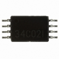
CAT34C02YI-G ON Semiconductor, CAT34C02YI-G Datasheet - Page 8

CAT34C02YI-G
Manufacturer Part Number
CAT34C02YI-G
Description
IC EEPROM 2KBIT 400KHZ 8TSSOP
Manufacturer
ON Semiconductor
Datasheet
1.CAT34C02VP2I-GT4.pdf
(14 pages)
Specifications of CAT34C02YI-G
Format - Memory
EEPROMs - Serial
Memory Type
EEPROM
Memory Size
2K (256 x 8)
Speed
400kHz
Interface
I²C, 2-Wire Serial
Voltage - Supply
1.7 V ~ 5.5 V
Operating Temperature
-40°C ~ 85°C
Package / Case
8-TSSOP
Organization
256 K x 8
Interface Type
I2C
Maximum Clock Frequency
0.4 MHz
Access Time
900 ns
Supply Voltage (max)
5.5 V
Supply Voltage (min)
1.7 V
Maximum Operating Current
1 mA
Maximum Operating Temperature
+ 85 C
Mounting Style
SMD/SMT
Minimum Operating Temperature
- 40 C
Operating Supply Voltage
1.8 V , 2.5 V , 3.3 V , 5 V
Lead Free Status / RoHS Status
Lead free / RoHS Compliant
Other names
34C02YI-G
Available stocks
Company
Part Number
Manufacturer
Quantity
Price
Company:
Part Number:
CAT34C02YI-GT3
Manufacturer:
CATALYST
Quantity:
5 388
Part Number:
CAT34C02YI-GT3
Manufacturer:
CATALYST
Quantity:
20 000
Company:
Part Number:
CAT34C02YI-GT5
Manufacturer:
ON Semiconductor
Quantity:
3 950
Software Write Protection
protected against Write requests by setting one of two
Software Write Protection (SWP) flags.
can be set or read while all address pins are at regular CMOS
levels (GND or V
must be present on address pin A
Reversible Software Write Protection (RSWP) flag. The
D.C. OPERATING CONDITIONS for RSWP operations
are shown in Table 8.
are preceded by a START and terminated with a STOP,
following the ACK or NoACK from the CAT34C02. All
SWP related Slave addresses use the pre−amble: 0110 (6h),
instead of the regular 1010 (Ah) used for memory access.
For PSWP commands, the three address pins can be at any
logic level, whereas for RSWP commands the address pins
must be at pre−assigned logic levels. V
logic ‘1’. The V
before the START and maintained just beyond the STOP.
Otherwise an RSWP request could be interpreted by the
CAT34C02 as a PSWP request.
convention, i.e. to read the state of the SWP flag, the LSB of
the Slave address must be ‘1’, and to set or clear a flag, it
must be ‘0’. For Write commands a dummy byte address and
dummy data byte must be provided (Figure 14). In contrast
to a regular memory Read, a SWP Read does not return Data.
Instead the CAT34C02 will respond with NoACK if the flag
11. To prevent damaging the CAT34C02 while applying V
Table 8. RSWP D.C. OPERATING CONDITIONS
The lower half of memory (first 128 bytes) can be
The Permanent Software Write Protection (PSWP) flag
The SWP commands are listed in Table 9. All commands
The SWP Slave addresses follow the standard I
Symbol
resistor (> 1.5 kW) between the supply and the input pin. The resistance is only limited by the combination of V
the resistor can be omitted if V
As an example: V
DV
I
V
HVD
I
HV
HV
HV
A
A
A
A
0
0
0
0
HV
Overdrive (V
High Voltage Detector Current
Very High Voltage
Input Current @ V
CC
CC
condition must be established on pin A
), whereas the very high voltage V
= 1.7 V, V
HV
Parameter
HV
HV
− V
HV
is clamped well below 10 V, it nevertheless provides simple protection against EOS events.
= 8 V, 1.5 kW < R
CC
0
to set, clear or read the
)
HV
is interpreted as
S
HV
< 15 kW.
, it is strongly recommended to limit the power delivered to pin A
(Note 11)
http://onsemi.com
HV
2
C
0
8
is set and with ACK if the flag is not set. Therefore, the
Master can immediately follow up with a STOP, as there is
no meaningful data following the ACK interval (Figure 15).
Hardware Write Protection
as the SWP flags are protected against Write operations, see
Memory Protection Map below. If the WP pin is left floating
or is grounded, it has no impact on the operation of the
CAT34C02.
of SCL immediately preceding the first data byte (Figure 9).
If the WP pin is HIGH during the strobe interval, the
CAT34C02 will not acknowledge the data byte and the Write
request will be rejected.
1.7 V < V
FFH
7FH
00H
Test Conditions
With the WP pin held HIGH, the entire memory, as well
The state of the WP pin is strobed on the last falling edge
CC
Figure 13. Memory Protection Map
< 3.6 V
Min
4.8
Hardware Write Protectable
(by connecting WP pin to
V
7
Software Write Protectable
(by setting the write
protect flags)
CC
HV
)
and maximum I
0
, by inserting a series
Max
0.1
10
1
HVD
Units
mA
mA
. While
V
V


