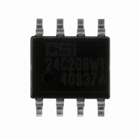
CAT24C208WI-G ON Semiconductor, CAT24C208WI-G Datasheet

CAT24C208WI-G
Specifications of CAT24C208WI-G
Available stocks
Related parts for CAT24C208WI-G
CAT24C208WI-G Summary of contents
Page 1
... CAT24C208 features a 16−byte page write buffer and can be accessed 2 from either of two separate I C compatible ports, DSP (SDA, SCL) and DDC (SDA, SCL). Arbitration between the two interface ports is automatic and allows the appearance of individual access to the memory from each interface. Features • 2 Supports Standard and Fast I C Protocol • ...
Page 2
... DDC SDA pin, and is used to block DDC Port for access when DSP Port is active. 7 EDID SEL EDID select. The CAT24C208 EDID select input selects the active bank of memory to be accessed via the DDC SDA/SCL interface as set in the configuration register. 8 DDC V Device power when powered from a DDC host ...
Page 3
Table 5. D.C. OPERATING CHARACTERISTICS Symbol Parameter I Power Supply Current CC I Standby Current ( Input Leakage Current LI I Output Leakage Current LO V Input Low Voltage IL V Input High Voltage ...
Page 4
... Each bank of memory can be used to store an E−EDID (DDC_SDA and data structure. However, only one bank can be read through the DDC port at a time. The active bank of memory (that is, the bank that appears at address A0h on the DDC port) is controlled through the configuration register at 62/63h and the EDID_SEL pin. ...
Page 5
... C bus serial interface. All memory space operations are done at the A0/A1 DDC address pair. As such, all write operations to the memory space are done at DDC address A0h and all read operations of the memory space are done at DDC address A1h. Figure 6 shows the bit sequence of a random read from anywhere within the memory space ...
Page 6
... ACK A7 − A0 ADDRESS The segment pointer is at the address 60h and is write−only. This means that a memory access at 61h will give undefined results. The segment pointer is a volatile register. The device configuration register at 62/63 (hex non−volatile register. The configuration register will be shipped in the erased (set to FFh) state ...
Page 7
... DSP Interface 2 The DSP interface is similar bus serial interface. Without the segment pointer, the maximum accessible memory space is 256 bytes of segment 00h only. In the START 1010 0000 ACK A7 − A0 ADDRESS START 1010 0000 ACK A7 − A0 ADDRESS ACK START 1010 0001 START ...
Page 8
... When a START condition is detected on Table 9. CONFIGURATION REGISTER Register Function Configuration Register Function Description NB: Number of memory banks in DDC port memory map Banks Bank AB0: Active Bank Control Bit 0 (See Table 10) AB1: Active Bank Control Bit 1 (See Table 10) WE DDC: Write Enable 0 = Write Disabled, 1= Write Enabled (Note 8) 8 ...
Page 9
PIN # 1 IDENTIFICATION TOP VIEW SIDE VIEW Notes: (1) All dimensions are in millimeters. Angles in degrees. (2) Complies with JEDEC MS-012. PACKAGE DIMENSIONS SOIC 8, 150 mils CASE 751BD−01 ISSUE O SYMBOL ...
Page 10
... All packages are RoHS-compliant (Lead-free, Halogen-free). 10. The standard lead finish is NiPdAu. 11. The device used in the above example is a CAT24C208WI−GT3 (SOIC, Industrial Temperature, NiPdAu, Tape & Reel). 12. For additional package and temperature options, please contact your nearest ON Semiconductor Sales office. 13. For information on tape and reel specifications, including part orientation and tape sizes, please refer to our Tape and Reel Packaging Specifications Brochure, BRD8011/D ...


