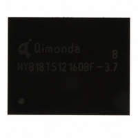
HYB18T1G160BF-5 Qimonda, HYB18T1G160BF-5 Datasheet - Page 24

HYB18T1G160BF-5
Manufacturer Part Number
HYB18T1G160BF-5
Description
IC DDR2 SDRAM 1GBIT 84TFBGA
Manufacturer
Qimonda
Datasheet
1.HYB18T1G800BF-3S.pdf
(74 pages)
Specifications of HYB18T1G160BF-5
Format - Memory
RAM
Memory Type
DDR2 SDRAM
Memory Size
1G (64M x 16)
Speed
200MHz
Interface
Parallel
Voltage - Supply
1.7 V ~ 1.9 V
Operating Temperature
0°C ~ 95°C
Package / Case
84-TFBGA
Lead Free Status / RoHS Status
Lead free / RoHS Compliant
Other names
675-1018-2
1) w = write only register bits
2) Number of clock cycles for write recovery during auto-precharge. WR in clock cycles is calculated by dividing t
Rev. 1.3, 2007-07
03062006-ZNH8-HURV
Field
CL
BT
BL
Field
BA2
BA1
BA0
A13
Qoff
rounding up to the next integer: WR [cycles] ≥ t
for the analogue t
Bits
[6:4]
3
[2:0]
Bits
16
15
14
13
12
Type
w
w
w
WR
Type
reg. addr.
w
w
timing WR
1)
1)
MIN
Description
CAS Latency
Note: All other bit combinations are illegal.
011
100
101
110
111
Burst Type
0
1
Burst Length
Note: All other bit combinations are illegal.
010
011
Description
Bank Address [2]
Note: BA2 not available on 256 Mbit and 512 Mbit components
0
Bank Address [1]
0
Bank Address [0]
1
Address Bus [13]
Note: A13 is not available for 256 Mbit and x16 512 Mbit configuration
0
Output Disable
0
1
B
B
is determined by t
B
B
B
B
B
B
B
B
B
B
B
B
B
CL 3
CL 4
CL 5
CL 6
CL 7
BT Sequential
BT Interleaved
BL 4
BL 8
BA2 Bank Address
BA1 Bank Address
BA0 Bank Address
A13 Address bit 13
QOff Output buffers enabled
QOff Output buffers disabled
WR
(ns) / t
CK.MAX
CK
(ns). The mode register must be programmed to fulfill the minimum requirement
and WR
24
Extended Mode Register Definition (BA[2:0] = 001
MAX
is determined by t
1-Gbit Double-Data-Rate-Two SDRAM
CK.MIN
HY[B/I]18T1G[40/80/16]0B[C/F](L/V)
.
WR
Internet Data Sheet
(in ns) by t
TABLE 20
CK
(in ns) and
B
)


