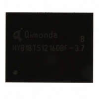
HYB18T1G160BF-5 Qimonda, HYB18T1G160BF-5 Datasheet - Page 33

HYB18T1G160BF-5
Manufacturer Part Number
HYB18T1G160BF-5
Description
IC DDR2 SDRAM 1GBIT 84TFBGA
Manufacturer
Qimonda
Datasheet
1.HYB18T1G800BF-3S.pdf
(74 pages)
Specifications of HYB18T1G160BF-5
Format - Memory
RAM
Memory Type
DDR2 SDRAM
Memory Size
1G (64M x 16)
Speed
200MHz
Interface
Parallel
Voltage - Supply
1.7 V ~ 1.9 V
Operating Temperature
0°C ~ 95°C
Package / Case
84-TFBGA
Lead Free Status / RoHS Status
Lead free / RoHS Compliant
Other names
675-1018-2
5.2
Input and output 0s are higher with dual-die components compared to standard single-die components, due to the double
loading of the input / output pins, except CS[1:0], CKE[1:0] and ODT[1:0] and the additional package internal wiring.
1)
2) The value of
3) Peak to peak ac noise on
4)
1)
2) Measurement Definition for
1) All other pins not under test = 0 V
2) DQ’s, LDQS, LDQS, UDQS, UDQS, DQS, DQS, RDQS, RDQS are disabled and ODT is turned off
Rev. 1.3, 2007-07
03062006-ZNH8-HURV
Symbol
V
V
V
V
V
Parameter / Condition
Termination resistor impedance value for
EMRS(1)[A6,A2] = [0,1]; 75 Ohm
Termination resistor impedance value for
EMRS(1)[A6,A2] =[1,0]; 150 Ohm
Termination resistor impedance value for
EMRS(1)(A6,A2)=[1,1]; 50 Ohm
Deviation of
Symbol
I
I
IL
OL
DD
DDDL
DDQ
REF
TT
V
be about 0.5 ×
V
must track variations in die dc level of
Rtt(eff) = (
Measurement Definition for Rtt(eff): Apply
1) x 100 %
DDQ
TT
is not applied directly to the device.
tracks with
V
V
IH(ac)
Parameter / Condition
Input Leakage Current; any input 0 V <
Output Leakage Current; 0 V <
M
V
Parameter
Supply Voltage
Supply Voltage for DLL
Supply Voltage for Output
Input Reference Voltage
Termination Voltage
REF
with respect to
V
DDQ
–
V
may be selected by the user to provide optimum noise margin in the system. Typically the value of
DD
V
DC Characteristics
IL(ac)
,
of the transmitting device and
V
DDDL
) /(
V
I
(
REF
V
tracks with
V
M
IHac
: Turn ODT on and measure voltage (
may not exceed ± 2 %
V
) –
DDQ
I
(
V
V
/ 2
ILac
V
REF
V
DD
TT
)).
.
V
. AC parameters are measured with
is a system supply for signal termination resistors, is expected to be set equal to
IH(ac)
V
and
OUT
V
Rating
1.7
1.7
1.7
0.49 ×
V
REF
Min.
REF
V
<
V
IL(ac)
REF
is expected to track variations in
V
V
– 0.04
DDQ
IN
Symbol
Rtt1(eff)
Rtt2(eff)
Rtt3(eff)
delta
V
(dc)
to test pin separately, then measure current
<
DDQ
V
33
DD
V
Recommended DC Operating Conditions (SSTL_18)
M
V
M
) at test pin (midpoint) with no load: delta
Typ.
1.8
1.8
0.5 ×
V
1.8
REF
Min.
60
120
40
–6.00
V
V
DDQ
DD
,
V
DDQ
1-Gbit Double-Data-Rate-Two SDRAM
Nom.
75
150
50
—
Input and Output Leakage Currents
V
ODT DC Electrical Characteristics
Min.
–2
–5
and
DDQ
HY[B/I]18T1G[40/80/16]0B[C/F](L/V)
Max.
1.9
1.9
1.9
0.51 ×
V
REF
.
V
DDDL
+ 0.04
V
Max.
90
180
60
+ 6.00
tied together.
DDQ
Max.
+2
+5
I
(
V
IHac
) and
Internet Data Sheet
V
Unit
Ω
Ω
Ω
%
Unit
V
V
V
V
V
M
Unit
µA
µA
I
= ((2 x
V
(
TABLE 30
TABLE 31
TABLE 32
V
REF
ILac
is expected to
) respectively.
V
V
Note
1)
1)
1)
2)3)
4)
Note
1)
1)
1)
2)
M
REF
Note
1)
2)
/
V
, and
DDQ
) –


