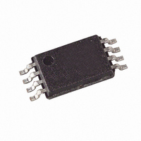
AT24HC02B-TH-B Atmel, AT24HC02B-TH-B Datasheet - Page 10

AT24HC02B-TH-B
Manufacturer Part Number
AT24HC02B-TH-B
Description
IC EEPROM 2KBIT 1MHZ 8TSSOP
Manufacturer
Atmel
Specifications of AT24HC02B-TH-B
Format - Memory
EEPROMs - Serial
Memory Type
EEPROM
Memory Size
2K (256 x 8)
Speed
400kHz, 1MHz
Interface
I²C, 2-Wire Serial
Voltage - Supply
1.8 V ~ 5.5 V
Operating Temperature
-40°C ~ 85°C
Package / Case
8-TSSOP
Organization
256 K x 8
Interface Type
2-Wire
Maximum Clock Frequency
0.4 MHz
Access Time
900 ns
Supply Voltage (max)
5.5 V
Supply Voltage (min)
1.8 V
Maximum Operating Current
3 mA
Maximum Operating Temperature
+ 85 C
Mounting Style
SMD/SMT
Minimum Operating Temperature
- 40 C
Operating Supply Voltage
1.8 V, 5.5 V
Capacitance, Input
6 pF
Capacitance, Output
8 pF
Current, Input, Leakage
0.1 μA
Current, Operating
0.4 mA (Read), 2 mA (Write)
Current, Output, Leakage
0.05
Data Retention
100 yrs.
Density
2K
Package Type
TSSOP
Temperature, Operating
-40 to +85 °C
Time, Access
0.55 μs
Time, Fall
300 ns
Time, Rise
0.3 μs
Voltage, Input, High
2.3 to 6 V
Voltage, Input, Low
0.54 to 1.65 V
Voltage, Output, Low
0.2 V
Voltage, Supply
1.8 to 5.5 V
Lead Free Status / RoHS Status
Lead free / RoHS Compliant
Other names
AT24HC02B-10TU-1.8
AT24HC02B-10TU-1.8
AT24HC02B-10TU-1.8
8. Read Operations
10
AT24HC02B
Read operations are initiated the same way as write operations with the exception that the
read/write select bit in the device address word is set to “1”. There are three read operations:
current address read, random address read and sequential read.
CURRENT ADDRESS READ: The internal data word address counter maintains the last
address accessed during the last read or write operation, incremented by one. This address
stays valid between operations as long as the chip power is maintained. The address “roll over”
during read is from the last byte of the last memory page to the first byte of the first page. The
address “roll over” during write is from the last byte of the current page to the first byte of the
same page.
Once the device address with the read/write select bit set to “1” is clocked in and acknowledged
by the EEPROM, the current address data word is serially clocked out. The microcontroller does
not respond with an input “0” but does generate a following stop condition, see
Figure 8-1.
RANDOM READ: A random read requires a “dummy” byte write sequence to load in the data
word address. Once the device address word and data word address are clocked in and
acknowledged by the EEPROM, the microcontroller must generate another start condition. The
microcontroller now initiates a current address read by sending a device address with the
read/write select bit high. The EEPROM acknowledges the device address and serially clocks
out the data word. The microcontroller does not respond with a “0” but does generate a following
stop condition, see
Figure 8-2.
SDA LINE
Current Address Read
Random Read
S
A
R
T
T
M
S
B
Figure
ADDRESS
SDA LINE
DEVICE
8-2.
DUMMY WRITE
W
W
R
T
E
R
I
/
S
T
A
R
T
C
A
K
M
S
B
M
S
B
ADDRESS
DEVICE
ADDRESS n
WORD
W
R
D
R
E
A
/
A
C
K
A
C
K
S
T
A
R
T
M
S
B
ADDRESS
DEVICE
DATA
R
E
A
D
A
C
K
N
O
A
C
K
O
S
T
P
DATA n
Figure
5134E–SEEPR–3/08
8-1.
N
O
A
C
K
S
O
P
T


