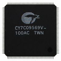
CY7C09569V-100AC Cypress Semiconductor Corp, CY7C09569V-100AC Datasheet - Page 11

CY7C09569V-100AC
Manufacturer Part Number
CY7C09569V-100AC
Description
IC SRAM 576KBIT 100MHZ 144LQFP
Manufacturer
Cypress Semiconductor Corp
Specifications of CY7C09569V-100AC
Format - Memory
RAM
Memory Type
SRAM - Dual Port, Synchronous
Memory Size
576K (16K x 36)
Speed
100MHz
Interface
Parallel
Voltage - Supply
3 V ~ 3.6 V
Operating Temperature
0°C ~ 70°C
Package / Case
144-LQFP
Density
576Kb
Access Time (max)
12.5ns
Sync/async
Synchronous
Architecture
SDR
Clock Freq (max)
67MHz
Operating Supply Voltage (typ)
3.3V
Address Bus
14b
Package Type
TQFP
Operating Temp Range
0C to 70C
Number Of Ports
2
Supply Current
385mA
Operating Supply Voltage (min)
3.135V
Operating Supply Voltage (max)
3.465V
Operating Temperature Classification
Commercial
Mounting
Surface Mount
Pin Count
144
Word Size
36b
Number Of Words
16K
Lead Free Status / RoHS Status
Contains lead / RoHS non-compliant
Other names
428-1189
Available stocks
Company
Part Number
Manufacturer
Quantity
Price
Company:
Part Number:
CY7C09569V-100AC
Manufacturer:
Cypress Semiconductor Corp
Quantity:
10 000
Part Number:
CY7C09569V-100AC
Manufacturer:
CYP
Quantity:
20 000
Switching Waveforms
Bus Match Read Cycle for Flow-Through Output (FT/PIPE = V
Bus Match Read Cycle for Pipelined Operation (FT/PIPE = V
Notes:
Document #: 38-06054 Rev. *A
14. Timing shown is for x18 bus matching; x9 bus matching is similar with 4 cycles between address inputs.
15. See table “Right Port Operation“for data output on first and subsequent cycles.
16. CNTEN = V
ADDRESS
DATA
DATA
ADDRESS
level all the time except when loading the initial external address (i.e. ADS = V
ADS
ADS
CLK
R/W
OUT
OE
R/W
OUT
CLK
CE
OE
CE
LOW
IL
LOW
t
. In x9 and x18 Bus Matching Burst Mode operations (Write or Read), ADS can toggle on the rising edge of every clock cycle or it can be at V
t
t
t
SC
SC
SW
SA
t
t
SA
SW
A
A
n
n
t
t
HA
HW
t
CH2
t
t
t
t
t
HC
HW
HA
HC
CH1
t
CKLZ
(continued)
t
CYC2
t
CD1
t
CYC1
1 Latency
t
CL2
t
CL1
A
n
t
CLKZ
A
n
Cycle
t
DC
1st
Q
t
CD2
n
1st Cycle
IH
A
IL
IL
)
n+1
Q
[10, 12, 14, 15, 16]
only required when reading or writing the first Byte or Word).
)
n
[10, 12, 14, 15, 16]
t
A
DC
n+1
t
CD2
Cycle
Q
2nd
n
2nd Cycle
A
Q
n+1
n
t
DC
A
n+1
t
CD2
Cycle
Q
1st
t
DC
n+1
CY7C09569V
CY7C09579V
1st Cycle
Q
Page 11 of 30
n+1
t
DC
Cycle
Q
2nd
n+1
IH


