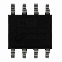
CAT24C128WI-G ON Semiconductor, CAT24C128WI-G Datasheet

CAT24C128WI-G
Specifications of CAT24C128WI-G
Available stocks
Related parts for CAT24C128WI-G
CAT24C128WI-G Summary of contents
Page 1
... Figure 1. Functional Symbol *For additional information on our Pb−Free strategy and soldering details, please download the ON Semiconductor Soldering and Mounting Techniques Reference Manual, SOLDERRM/D. © Semiconductor Components Industries, LLC, 2009 September, 2009 − Rev protocol Bus Inputs SOIC−8 W SUFFIX CASE 751BD ...
Page 2
Table 1. ABSOLUTE MAXIMUM RATINGS Storage Temperature Voltage on Any Pin with Respect to Ground (Note 1) Stresses exceeding Maximum Ratings may damage the device. Maximum Ratings are stress ratings only. Functional operation above the Recommended Operating Conditions is not ...
Page 3
Table 5. A.C. CHARACTERISTICS Symbol F Clock Frequency SCL t START Condition Hold Time HD:STA t Low Period of SCL Clock LOW t High Period of SCL Clock HIGH t START Condition Setup Time SU:STA t Data Hold Time HD:DAT ...
Page 4
Power−On Reset (POR) The CAT24C128 incorporates Power−On Reset (POR) circuitry which protects the device against powering up in the wrong state. The CAT24C128 will power up into Standby mode after V exceeds the POR trigger level and will power down ...
Page 5
SCL SDA START CONDITION BUS RELEASE DELAY (TRANSMITTER) SCL FROM MASTER DATA OUTPUT FROM TRANSMITTER DATA OUTPUT FROM RECEIVER START t F SCL t SU:STA t SDA IN SDA OUT Figure 2. START/STOP Conditions DEVICE ADDRESS ...
Page 6
... A byte following the address bytes will be interpreted as data. The data will be loaded into the Page Write Buffer and will eventually be written to memory at the address specified by the 14 active address bits provided earlier. The CAT24C128 will acknowledge the Slave address, address bytes and data byte. ...
Page 7
... Master responds with a NoACK, followed by a STOP (Figure 12). In contrast to Page Write, during Sequential Read the address count will automatically increment to and then wrap−around at end of memory (rather than end of page). http://onsemi.com 7 DATA DATA ...
Page 8
BUS ACTIVITY: MASTER SLAVE SCL SDA Figure 10. Immediate Read Sequence and Timing BUS ACTIVITY SLAVE R MASTER ADDRESS SLAVE Don’t Care Bit BUS ACTIVITY: SLAVE MASTER ADDRESS A SLAVE ...
Page 9
PIN # 1 IDENTIFICATION D TOP VIEW SIDE VIEW Notes: (1) All dimensions are in millimeters. (2) Complies with JEDEC MS-001. PACKAGE DIMENSIONS PDIP−8, 300 mils CASE 646AA−01 ISSUE A SYMBOL ...
Page 10
PIN # 1 IDENTIFICATION TOP VIEW SIDE VIEW Notes: (1) All dimensions are in millimeters. Angles in degrees. (2) Complies with JEDEC MS-012. PACKAGE DIMENSIONS SOIC 8, 150 mils CASE 751BD−01 ISSUE O SYMBOL ...
Page 11
E1 e TOP VIEW SIDE VIEW Notes: (1) All dimensions are in millimeters. Angles in degrees. (2) Complies with JEDEC MO-153. PACKAGE DIMENSIONS TSSOP8, 4.4x3 CASE 948AL−01 ISSUE O SYMBOL MIN A A1 0.05 A2 ...
Page 12
D E PIN #1 INDEX AREA TOP VIEW SYMBOL MIN NOM A 0.45 0.50 A1 0.00 0.02 A3 0.127 REF b 0.20 0.25 D 1.90 2.00 D2 1.50 1.60 E 2.90 3.00 E2 0.10 0.20 e 0.50 TYP K 0.10 ...
Page 13
E E1 TOP VIEW SIDE VIEW Notes: (1) All dimensions are in millimeters. Angles in degrees. (2) Complies with JEDEC MO-187. PACKAGE DIMENSIONS MSOP 8, 3x3 CASE 846AD−01 ISSUE O SYMBOL MIN A A1 ...
Page 14
... For information on tape and reel specifications, including part orientation and tape sizes, please refer to our Tape and Reel Packaging Specifications Brochure, BRD8011/D. ORDERABLE PART NUMBERS Order Number CAT24C128LI−G CAT24C128WI−GT3 CAT24C128YI−GT3 CAT24C128HU3IGT3* CAT24C128ZI−GT3 *Part number is not exactly the same as the “Example of Ordering Information” shown above. ...


