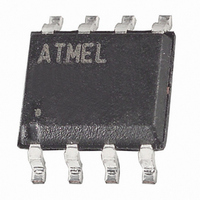
AT25DF321A-SH-B Atmel, AT25DF321A-SH-B Datasheet - Page 32

AT25DF321A-SH-B
Manufacturer Part Number
AT25DF321A-SH-B
Description
IC FLASH 32MBIT 100MHZ 8SOIC
Manufacturer
Atmel
Datasheet
1.AT25DF321A-SH-T.pdf
(51 pages)
Specifications of AT25DF321A-SH-B
Format - Memory
FLASH
Memory Type
DataFLASH
Memory Size
32M (16384 pages x 256 Bytes)
Speed
100MHz
Interface
SPI, RapidS
Voltage - Supply
2.7 V ~ 3.6 V
Operating Temperature
-40°C ~ 85°C
Package / Case
8-SOIC (5.3mm Width), 8-SOP, 8-SOEIAJ
Memory Configuration
16384 Pages X 256 Bytes
Interface Type
Serial, SPI
Clock Frequency
100MHz
Supply Voltage Range
2.7V To 3.6V
Memory Case Style
SOIC
Rohs Compliant
Yes
Lead Free Status / RoHS Status
Lead free / RoHS Compliant
11.1.3 WPP Bit
11.1.4 SWP Bits
11.1.5 WEL Bit
11.1.6 RSTE Bit
32
The WPP bit can be read to determine if the WP pin has been asserted or not.
The SWP bits provide feedback on the software protection status for the device. There are three possible combinations of
the SWP bits that indicate whether none, some, or all of the sectors have been protected using the Protect Sector
command or the Global Protect feature. If the SWP bits indicate that some of the sectors have been protected, then the
individual Sector Protection Registers can be read with the Read Sector Protection Registers command to determine which
sectors are in fact protected.
The WEL bit indicates the current status of the internal Write Enable Latch. When the WEL bit is in the logical “0” state,
the device will not accept any Byte/Page Program, erase, Protect Sector, Unprotect Sector, Sector Lockdown, Freeze
Sector Lockdown State, Program OTP Security Register, or Write Status Register commands. The WEL bit defaults to the
logical “0” state after a device power-up or reset operation. In addition, the WEL bit will be reset to the logical “0” state
automatically under the following conditions:
If the WEL bit is in the logical “1” state, it will not be reset to a logical “0” if an operation aborts due to an incomplete or
unrecognized opcode being clocked into the device before the CS pin is deasserted. In order for the WEL bit to be reset
when an operation aborts prematurely, the entire opcode for a Byte/Page Program, erase, Protect Sector, Unprotect
Sector, Sector Lockdown, Freeze Sector Lockdown State, Program OTP Security Register, or Write Status Register
command must have been clocked into the device.
The RSTE bit is used to enable or disable the Reset command. When the RSTE bit is in the logical “0” state (the default
state after power-up), the Reset command is disabled and any attempts to reset the device using the Reset command will
be ignored. When the RSTE bit is in the logical “1” state, the Reset command is enabled.
The RSTE bit will retain its state as long as power is applied to the device. Once set to the logical “1” state, the RSTE bit
will remain in that state until it is modified using the Write Status Register Byte 2 command or until the device has been
power cycled. The Reset command itself will not change the state of the RSTE bit.
•
•
•
•
•
•
•
•
•
•
•
Atmel AT25DF321A
Write Disable operation completes successfully
Write Status Register operation completes successfully or aborts
Protect Sector operation completes successfully or aborts
Unprotect Sector operation completes successfully or aborts
Sector Lockdown operation completes successfully or aborts
Freeze Sector Lockdown State operation completes successfully or aborts
Program OTP Security Register operation completes successfully or aborts
Byte/Page Program operation completes successfully or aborts
Block Erase operation completes successfully or aborts
Chip Erase operation completes successfully or aborts
Hold condition aborts
3686D–DFLASH–12/09


