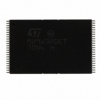
M29W320ET70N6E NUMONYX, M29W320ET70N6E Datasheet - Page 23

M29W320ET70N6E
Manufacturer Part Number
M29W320ET70N6E
Description
IC FLASH 32MBIT 70NS 48TSOP
Manufacturer
NUMONYX
Series
Axcell™r
Specifications of M29W320ET70N6E
Format - Memory
FLASH
Memory Type
FLASH - Nor
Memory Size
32M (4Mx8, 2Mx16)
Speed
70ns
Interface
Parallel
Voltage - Supply
2.7 V ~ 3.6 V
Operating Temperature
-40°C ~ 85°C
Package / Case
48-TSOP
Supply Voltage Range
2.7V To 3.6V
Memory Case Style
TSOP
No. Of Pins
48
Access Time
70ns
Base Number
29
Ic Generic Number
29W320
Memory Configuration
4M X 8, 2M X 16
Interface Type
CFI, Parallel
Rohs Compliant
Yes
Lead Free Status / RoHS Status
Lead free / RoHS Compliant
Other names
497-3608
497-3608
497-3608
Available stocks
Company
Part Number
Manufacturer
Quantity
Price
Company:
Part Number:
M29W320ET70N6E
Manufacturer:
MICRON
Quantity:
15 600
Company:
Part Number:
M29W320ET70N6E
Manufacturer:
Numonyx
Quantity:
23 040
Part Number:
M29W320ET70N6E
Manufacturer:
ST
Quantity:
20 000
M29W320ET, M29W320EB
4.6
4.7
4.8
4.9
Unlock Bypass command
The Unlock Bypass command is used in conjunction with the Unlock Bypass Program
command to program the memory faster than with the standard program commands. When
the cycle time to the device is long, considerable time saving can be made by using these
commands. Three Bus Write operations are required to issue the Unlock Bypass command.
Once the Unlock Bypass command has been issued the memory enters Unlock Bypass
mode. The Unlock Bypass Program command can then be issued to program addresses or
the Unlock Bypass Reset command can be issued to return to Read mode. In Unlock
Bypass mode the memory can be read as if in Read mode.
When V
Unlock Bypass mode and the Unlock Bypass Program command can be issued
immediately. Care must be taken because applying a 12V V
will temporarily unprotect any protected block.
Unlock Bypass Program command
The Unlock Bypass Program command can be used to program one address in the memory
array at a time. The command requires two Bus Write operations, the final write operation
latches the address and data, and starts the Program/Erase Controller.
The Program operation using the Unlock Bypass Program command behaves identically to
the Program operation using the Program command. The operation cannot be aborted, a
Bus Read operation outputs the Status register. See the Program command for details on
the behavior.
Unlock Bypass Reset command
The Unlock Bypass Reset command can be used to return to Read/Reset mode from
Unlock Bypass mode. Two Bus Write operations are required to issue the Unlock Bypass
Reset command. Read/Reset command does not exit from Unlock Bypass mode.
Chip Erase command
The Chip Erase command can be used to erase the entire chip. Six Bus Write operations
are required to issue the Chip Erase Command and start the Program/Erase Controller.
If any blocks are protected then these are ignored and all the other blocks are erased. If all
of the blocks are protected the Chip Erase operation appears to start but will terminate
within about 100µs, leaving the data unchanged. No error condition is given when protected
blocks are ignored.
During the erase operation the memory will ignore all commands, including the Erase
Suspend command. It is not possible to issue any command to abort the operation. Typical
chip erase times are given in
operation will output the Status register on the Data Inputs/Outputs. See the section on the
Status register for more details.
After the Chip Erase operation has completed the memory will return to the Read mode,
unless an error has occurred. When an error occurs the memory will continue to output the
PP
is applied to the V
PP
Table
/Write Protect pin the memory automatically enters the
6. All Bus Read operations during the Chip Erase
PP
voltage to the VPP/WP pin
Command interface
23/63


