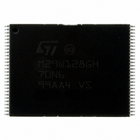
M29W128GH70N6E NUMONYX, M29W128GH70N6E Datasheet - Page 90

M29W128GH70N6E
Manufacturer Part Number
M29W128GH70N6E
Description
IC FLASH 128MBIT 70NS 56TSOP
Manufacturer
NUMONYX
Series
Axcell™r
Datasheet
1.M29W128GH70N6E.pdf
(94 pages)
Specifications of M29W128GH70N6E
Format - Memory
FLASH
Memory Type
FLASH
Memory Size
128M (16Mx8, 8Mx16)
Speed
70ns
Interface
Parallel
Voltage - Supply
2.7 V ~ 3.6 V
Operating Temperature
-40°C ~ 85°C
Package / Case
56-TSOP
Package
56TSOP
Cell Type
NOR
Density
128 Mb
Architecture
Sectored
Block Organization
Symmetrical
Typical Operating Supply Voltage
3|3.3 V
Sector Size
128KByte x 128
Timing Type
Asynchronous
Interface Type
Parallel
Lead Free Status / RoHS Status
Lead free / RoHS Compliant
Available stocks
Company
Part Number
Manufacturer
Quantity
Price
Company:
Part Number:
M29W128GH70N6E
Manufacturer:
Numonyx
Quantity:
17 280
Company:
Part Number:
M29W128GH70N6E
Manufacturer:
MICRON
Quantity:
595
Company:
Part Number:
M29W128GH70N6E
Manufacturer:
MICRON45
Quantity:
556
Part Number:
M29W128GH70N6E
Manufacturer:
ST
Quantity:
20 000
Appendix D
Figure 30. Write to buffer program flowchart and pseudocode
1. n+1 is the number of addresses to be programmed.
2. A write to buffer program abort and reset must be issued to return the device in read mode.
3. When the block address is specified, any address in the selected block address space is acceptable. However when
4. DQ7 must be checked since DQ5 and DQ7 may change simultaneously.
5. If this flowchart location is reached because DQ5=’1’, then the Write to Buffer Program command failed. If this flowchart
6. See
90/94
loading write buffer address with data, all addresses must fall within the selected write buffer page.
location is reached because DQ1=’1’, then the Write to Buffer Program command aborted. In both cases, the appropriate
reset command must be issued to return the device in read mode: a Reset command if the operation failed, a Write to
Buffer Program Abort and Reset command if the operation aborted.
Table 10
and
Table
11, for details on Write to Buffer Program command sequence.
Flowcharts
YES
NO
DQ1 = 1
NO
Write to Buffer Program
Confirm, block address
Check Status Register
Read Status Register
Program Address Pair
(DQ1, DQ5, DQ7) at
last loaded address
last loaded address
FAIL OR ABORT
Write Buffer Data,
(DQ5, DQ7) at
Write to Buffer
block address
block address
Write Next Data,
start address
DQ7 = Data
DQ7 = Data
Abort Write
command,
Write n
to Buffer
DQ5 = 1
X = X-1
X = 0
Start
YES
X=n
(4)
NO
NO
YES
NO
NO
(1)
,
(5)
YES
YES
(3)
YES
Program Aborted
Write to Buffer and
Write to a different
block address
Write to Buffer and Program command
END
First three cycles of the
(2)
AI08968b


