M48Z512AV-85PM1 STMicroelectronics, M48Z512AV-85PM1 Datasheet
M48Z512AV-85PM1
Specifications of M48Z512AV-85PM1
Available stocks


Related parts for M48Z512AV-85PM1


M48Z512AV-85PM1 Summary of contents
Page 1
... M48Z512AY: = 4.5 to 5.5 V, 4.2 V ≤ – M48Z512AV: = 3.0 to 3.6 V, 2.8 V ≤ M48Z512AV not for new design (see M48Z512BV). Contact ST sales office for availability. ■ Battery internally isolated until power is applied ■ Pin and function compatible with JEDEC standard 512 SRAMs ■ ...
Page 2
... Operating modes . . . . . . . . . . . . . . . . . . . . . . . . . . . . . . . . . . . . . . . . . . . . 7 2.1 READ mode . . . . . . . . . . . . . . . . . . . . . . . . . . . . . . . . . . . . . . . . . . . . . . . . 7 2.2 WRITE mode . . . . . . . . . . . . . . . . . . . . . . . . . . . . . . . . . . . . . . . . . . . . . . . 9 2.3 Data retention mode . . . . . . . . . . . . . . . . . . . . . . . . . . . . . . . . . . . . . . . . . 11 2.4 V noise and negative going transients . . . . . . . . . . . . . . . . . . . . . . . . . Maximum ratings . . . . . . . . . . . . . . . . . . . . . . . . . . . . . . . . . . . . . . . . . . . and AC parameters . . . . . . . . . . . . . . . . . . . . . . . . . . . . . . . . . . . . . . 14 5 Package mechanical data . . . . . . . . . . . . . . . . . . . . . . . . . . . . . . . . . . . . 17 6 Part numbering . . . . . . . . . . . . . . . . . . . . . . . . . . . . . . . . . . . . . . . . . . . . 18 7 Environmental information . . . . . . . . . . . . . . . . . . . . . . . . . . . . . . . . . . . 19 8 Revision history . . . . . . . . . . . . . . . . . . . . . . . . . . . . . . . . . . . . . . . . . . . 20 2/21 M48Z512A, M48Z512AY, M48Z512AV Doc ID 5146 Rev 8 ...
Page 3
... M48Z512A, M48Z512AY, M48Z512AV List of tables Table 1. Signal names . . . . . . . . . . . . . . . . . . . . . . . . . . . . . . . . . . . . . . . . . . . . . . . . . . . . . . . . . . . . 5 Table 2. Operating modes . . . . . . . . . . . . . . . . . . . . . . . . . . . . . . . . . . . . . . . . . . . . . . . . . . . . . . . . . 7 Table 3. READ mode AC characteristics . . . . . . . . . . . . . . . . . . . . . . . . . . . . . . . . . . . . . . . . . . . . . . 9 Table 4. WRITE mode AC characteristics . . . . . . . . . . . . . . . . . . . . . . . . . . . . . . . . . . . . . . . . . . . . 11 Table 5. Absolute maximum ratings . . . . . . . . . . . . . . . . . . . . . . . . . . . . . . . . . . . . . . . . . . . . . . . . . 13 Table 6. Operating and AC measurement conditions . . . . . . . . . . . . . . . . . . . . . . . . . . . . . . . . . . . . 14 Table 7. Capacitance . . . . . . . . . . . . . . . . . . . . . . . . . . . . . . . . . . . . . . . . . . . . . . . . . . . . . . . . . . . . 14 Table 8. DC characteristics Table 9. Power down/up AC characteristics . . . . . . . . . . . . . . . . . . . . . . . . . . . . . . . . . . . . . . . . . . . 16 Table 10. Power down/up trip points DC characteristics . . . . . . . . . . . . . . . . . . . . . . . . . . . . . . . . . . 16 Table 11. PMDIP32 – ...
Page 4
... WRITE enable controlled, WRITE AC waveforms . . . . . . . . . . . . . . . . . . . . . . . . . . . . . . . 10 Figure 7. Chip enable controlled, WRITE AC waveforms . . . . . . . . . . . . . . . . . . . . . . . . . . . . . . . . . 10 Figure 8. Supply voltage protection . . . . . . . . . . . . . . . . . . . . . . . . . . . . . . . . . . . . . . . . . . . . . . . . . . 12 Figure 9. AC measurement load circuit . . . . . . . . . . . . . . . . . . . . . . . . . . . . . . . . . . . . . . . . . . . . . . . 14 Figure 10. Power down/up mode AC waveforms Figure 11. PMDIP32 – 32-pin plastic DIP module, package outline . . . . . . . . . . . . . . . . . . . . . . . . . . 17 Figure 12. Recycling symbols . . . . . . . . . . . . . . . . . . . . . . . . . . . . . . . . . . . . . . . . . . . . . . . . . . . . . . . 19 4/21 M48Z512A, M48Z512AY, M48Z512AV Doc ID 5146 Rev 8 ...
Page 5
... M48Z512A, M48Z512AY, M48Z512AV 1 Device overview Figure 1. Logic diagram Table 1. Signal names A0-A18 DQ0-DQ7 A0-A18 M48Z512A W M48Z512AY M48Z512AV Address inputs Data inputs/outputs Chip enable input Output enable input WRITE enable input Supply voltage Ground Doc ID 5146 Rev 8 Device overview 8 DQ0-DQ7 AI02043 5/21 ...
Page 6
... A14 3 A12 M48Z512A A4 8 M48Z512AY A3 9 M48Z512AV DQ0 13 DQ1 14 DQ2 POWER VOLTAGE SENSE AND E SWITCHING CIRCUITRY INTERNAL BATTERY Doc ID 5146 Rev 8 M48Z512A, M48Z512AY, M48Z512AV A15 30 A17 A13 A11 A10 DQ7 20 DQ6 19 DQ5 18 DQ4 17 DQ3 A0-A18 DQ0-DQ7 512K x 8 SRAM ARRAY AI02044 ...
Page 7
... M48Z512A, M48Z512AY, M48Z512AV 2 Operating modes The M48Z512A/Y/V also has its own power-fail detect circuit. The control circuitry constantly monitors the single V tolerance, the circuit WRITE protects the SRAM, providing a high degree of data security in the midst of unpredictable system operation brought on by low V switchover voltage (V until valid power returns ...
Page 8
... Chip enable or output enable controlled, READ mode AC waveforms A0-A18 E G DQ0-DQ7 1. WRITE enable (W) = high Figure 5. Address controlled, READ mode AC waveforms A0-A18 DQ0-DQ7 1. Chip enable (E) and output enable (G) = low, WRITE enable (W) = high 8/21 M48Z512A, M48Z512AY, M48Z512AV tAVAV VALID tAVQV tELQV tELQX tGLQV tGLQX DATA OUT tAVAV tAVQV DATA VALID ...
Page 9
... M48Z512A, M48Z512AY, M48Z512AV Table 3. READ mode AC characteristics Symbol t READ cycle time AVAV t Address valid to output valid AVQV t Chip enable low to output valid ELQV t Output enable low to output valid GLQV (2) t Chip enable low to output transition ELQX (2) t Output enable low to output transition ...
Page 10
... Chip enable controlled, WRITE AC waveforms A0-A18 E W DQ0-DQ7 1. Output enable (G) = high. 10/21 tAVAV VALID tAVWH tAVEL tWLWH tAVWL tWLQZ tAVAV VALID tAVEH tAVEL tELEH tAVWL tDVEH Doc ID 5146 Rev 8 M48Z512A, M48Z512AY, M48Z512AV tWHAX tWHQX tWHDX DATA INPUT tDVWH tEHAX tEHDX DATA INPUT AI01222 AI01223 ...
Page 11
... M48Z512A, M48Z512AY, M48Z512AV Table 4. WRITE mode AC characteristics Symbol t WRITE cycle time AVAV t Address valid to WRITE enable low AVWL t Address valid to chip enable low AVEL t WRITE enable pulse width WLWH t Chip enable low to chip enable high ELEH t WRITE enable high to address transition ...
Page 12
... Figure 8. Supply voltage protection 12/21 bus. These transients can be reduced if CC that drive it to values below V CC (cathode connected 0.1µF Doc ID 5146 Rev 8 M48Z512A, M48Z512AY, M48Z512AV bus. The energy stored in the much anode (Schottky diode 1N5817 DEVICE V SS Figure 8) AI02169 ...
Page 13
... M48Z512A, M48Z512AY, M48Z512AV 3 Maximum ratings Stressing the device above the rating listed in the absolute maximum ratings table may cause permanent damage to the device. These are stress ratings only and operation of the device at these or any other conditions above those indicated in the operating sections of this specification is not implied ...
Page 14
... Figure 9. AC measurement load circuit 1. Excluding open drain output pins for M48Z512AV. Table 7. Capacitance Symbol C Input capacitance IN (3) C Input/output capacitance IO 1. Effective capacitance measured with power supply (M48Z512A/Y) or 3.3 V (M48Z512AV); sampled only, not 100% tested. 2. Outputs deselected °C. 14/21 Parameter ) Grade Grade 650Ω ...
Page 15
... M48Z512A, M48Z512AY, M48Z512AV Table 8. DC characteristics Sym Parameter (2) I Input leakage current LI (2) I Output leakage current LO I Supply current CC I Supply current (standby) TTL CC1 I Supply current (standby) CMOS CC2 V Input low voltage IL V Input high voltage IH V Output low voltage ...
Page 16
... CC PFD fall time of less than t may cause corruption of RAM data. FB (1)(2) Parameter M48Z512A M48Z512AY M48Z512AV M48Z512A/Y M48Z512AV . °C or – ° Doc ID 5146 Rev 8 M48Z512A, M48Z512AY, M48Z512AV Min Max 300 M48Z512A/Y 10 M48Z512AV 150 10 1 M48Z512A/Y 40 150 M48Z512AV 40 250 40 120 = 4.75 to 5.5 V, 4.5 to 5.5 V, ...
Page 17
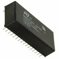
... M48Z512A, M48Z512AY, M48Z512AV 5 Package mechanical data In order to meet environmental requirements, ST offers these devices in different grades of ® ECOPACK packages, depending on their level of environmental compliance. ECOPACK specifications, grade definitions and product status are available at: www.st.com. ® ECOPACK trademark. Figure 11. PMDIP32 – 32-pin plastic DIP module, package outline 1 ...
Page 18
... Package PM = PMDIP32 Temperature range ° – °C 1. M48Z512AV not for new design (see M48Z512BV). Contact ST sales office for availability. For other options, or for more information on any aspect of this device, please contact the ST sales office nearest you. 18/21 M48Z512A, M48Z512AY, M48Z512AV M48Z 512AY – ...
Page 19
... M48Z512A, M48Z512AY, M48Z512AV 7 Environmental information Figure 12. Recycling symbols This product contains a non-rechargeable lithium (lithium carbon monofluoride chemistry) button cell battery fully encapsulated in the final product. Recycle or dispose of batteries in accordance with the battery manufacturer's instructions and local/national disposal and recycling regulations. Please refer to the following web site address for additional information regarding compliance statements and waste recycling www.st.com/nvram, then select " ...
Page 20
... ECOPACK package text added on coverpage. Note 2 concerning Leaded SOIC package removed below 6 Updated PMDIP32 package mechanical data in mechanical data; updated T 6 (-40 to 85°C). Indicated that M48Z512AV is Not for New Design; removed all ® 7 SNAPHAT battery and SOIC package references; updated Package mechanical data. ...
Page 21
... M48Z512A, M48Z512AY, M48Z512AV Information in this document is provided solely in connection with ST products. STMicroelectronics NV and its subsidiaries (“ST”) reserve the right to make changes, corrections, modifications or improvements, to this document, and the products and services described herein at any time, without notice. All ST products are sold pursuant to ST’s terms and conditions of sale. ...