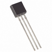
DS28EC20+ Maxim Integrated Products, DS28EC20+ Datasheet - Page 10

DS28EC20+
Manufacturer Part Number
DS28EC20+
Description
IC EEPROM 20KBIT TO92-3
Manufacturer
Maxim Integrated Products
Datasheet
1.DS28EC20PT.pdf
(27 pages)
Specifications of DS28EC20+
Format - Memory
EEPROMs - Serial
Memory Type
EEPROM
Memory Size
20K (256 x 80)
Interface
1-Wire Serial
Operating Temperature
-40°C ~ 85°C
Package / Case
TO-92-3 (Standard Body), TO-226
Lead Free Status / RoHS Status
Lead free / RoHS Compliant
Voltage - Supply
-
Speed
-
ADDRESS REGISTERS AND TRANSFER STATUS
The DS28EC20 employs three address registers: TA1, TA2, and E/S (Figure 6). Registers TA1 and TA2 must be
loaded with the target address to which the data is written or from which data is read. Register E/S is a read-only
transfer status register used to verify data integrity with write commands. ES bits E[4:0] are loaded with the
incoming T[4:0] on a Write Scratchpad command and increment on each subsequent data byte. This is, in effect, a
byte-ending offset counter within the 32-byte scratchpad. Bit 5 of the E/S register, called PF, is set if the number of
data bits sent by the master is not an integer multiple of 8 or if the data in the scratchpad is not valid due to a loss
of power. A valid write to the scratchpad clears the PF bit. Bit 6 has no function; it always reads 0. The highest
valued bit of the E/S register, called authorization accepted (AA), is valid only if the PF flag reads 0. If PF is 0 and
AA is 1, the data stored in the scratchpad has already been copied to the target memory address. Writing data to
the scratchpad clears this flag.
Figure 6. Address Registers
WRITING WITH VERIFICATION
To write data to the DS28EC20, the scratchpad must be used as intermediate storage. First, the master issues the
Write Scratchpad command to specify the desired target address, followed by the data to be written to the
scratchpad. Under certain conditions (see the Write Scratchpad Command section) the master receives an inverted
CRC16 of the command, address (actual address sent), and data at the end of the Write Scratchpad command
sequence. Knowing this CRC value, the master can compare it to the value it has calculated itself to decide if the
communication was successful and precede to the Copy Scratchpad command. If the master could not receive the
CRC16, it should send the Read Scratchpad command to verify data integrity. As a preamble to the scratchpad
data, the DS28EC20 repeats the target address TA1 and TA2 and sends the contents of the E/S register. If the PF
flag is set, data did not arrive correctly in the scratchpad or there was a loss of power since data was last written to
the scratchpad. The master does not need to continue reading; it can start a new trial to write data to the
scratchpad. Similarly, a set AA flag together with a cleared PF flag indicates that the device did not recognize the
Write command. If everything went correctly, both flags are cleared and the ending offset indicates the address of
the last byte written to the scratchpad. Now the master can continue reading and verifying every data byte. After
the master has verified the data, it can send the Copy Scratchpad command, for example. This command must be
followed exactly by the data of the three address registers TA1, TA2, and E/S. The master should obtain the
contents of these registers by reading the scratchpad. As soon as the DS28EC20 has received these bytes
correctly, it starts copying the scratchpad data to the requested location, provided that the target memory is not
copy protected, the PF flag is cleared, and there was no Read Memory or Extended Read Memory command
issued between Write Scratchpad and Copy Scratchpad.
Target Address (TA1)
Target Address (TA2)
Ending Address with
Data Status (E/S)
(Read Only)
Bit #
T15
AA
T7
7
T14
T6
6
0
T13
PF
T5
5
10 of 27
T12
T4
E4
4
T11
T3
E3
3
T10
T2
E2
2
T1
T9
E1
1
T0
T8
E0
0


