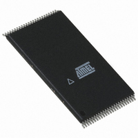
AT49F4096A-90TC Atmel, AT49F4096A-90TC Datasheet

AT49F4096A-90TC
Specifications of AT49F4096A-90TC
Available stocks
Related parts for AT49F4096A-90TC
AT49F4096A-90TC Summary of contents
Page 1
... Typical 10,000 Write Cycles Description The AT49F004(T) and AT49F4096A(T) are 5-volt, 4-megabit Flash Memories orga- nized as 524,288 words of 8 bits each or 256K words of 16 bits each. Manufactured with Atmel’s advanced nonvolatile CMOS technology, the devices offer access times with power dissipation of just 275 mW. When deselected, the CMOS standby current is less than 300 A. The device contains a user-enabled “ ...
Page 2
... The boot sector is designed to con- tain user secure code. For the AT49F4096A(T), the BYTE pin controls whether the device data I/O pins operate in the byte or word config- uration. If the BYTE pin is set at a logic “1” or left open, the device is in word configuration, I/O0 - I/O15 are active and controlled by CE and OE ...
Page 3
... AT49F004(T) Block Diagram V CC GND RESET ADDRESS INPUTS AT49F4096A(T) Block Diagram V CC GND RESET ADDRESS INPUTS Device Operation READ: The AT49F004(T)/4096A(T) is accessed like an EPROM. When CE and OE are low and WE is high, the data stored at the memory location determined by the address pins is asserted on the outputs. The outputs are put in the high impedance state whenever high ...
Page 4
... AT49F4096A; 7C002 for the AT49F004T; and 3E002H for the AT49F4096AT. If the data on I/O0 is low, the boot block can be programmed; if the data on I/O0 is high, the pro- gram lockout feature has been enabled and the block can- not be programmed ...
Page 5
For details, see Operating Modes (for hardware operation) or Software Product Identification. The manufacturer and device code is the same for both modes. DATA POLLING: The AT49F004(T)/4096A(T) features DATA polling to indicate the end of a program cycle. During a ...
Page 6
... The ADDRESS FORMAT in each bus cycle is as follows: A15 - A0 (Hex), A-1, and A15 - A18 (Don’t Care) 2. The boot sector has the address range 00000H to 03FFFH for the AT49F004; 7C000H to 7FFFFH for the AT49F004T; 00000H to 01FFFH for the AT49F4096A; and 3E000H to 3FFFFH for the AT49F4096AT. 3. Either one of the Product ID Exit commands can be used. ...
Page 7
... Software Notes can Refer to AC Programming Waveforms 12.0V 0.5V Manufacturer Code: 161FH Device Code: 11H (AT49F004), 1692H (AT49F4096A), 10H (AT49F004T), 1690H (AT49F4096AT). 5. See details under Software Product Identification Entry/Exit. DC Characteristics Symbol Parameter I Input Load Current LI I Output Leakage Current Standby Current CMOS ...
Page 8
AC Read Characteristics Symbol Parameter t Address to Output Delay ACC ( Output Delay CE ( Output Delay OE (3)( Output Float DF Output Hold from OE,CE or Address, ...
Page 9
AC Word Load Characteristics Symbol Parameter Address, OE Set-up Time AS OES t Address Hold Time AH t Chip Select Set-up Time CS t Chip Select Hold Time CH t Write Pulse Width (WE or CE) WP ...
Page 10
Program Cycle Characteristics Symbol Parameter t Byte/Word Programming Time BP t Address Set-up Time AS t Address Hold Time AH t Data Set-up Time DS t Data Hold Time DH t Write Pulse Width WP t Write Pulse Width High ...
Page 11
Data Polling Characteristics Symbol Parameter t Data Hold Time Hold Time OEH ( Output Delay OE t Write Recovery Time WR Notes: 1. These parameters are characterized and not 100% tested. 2. See t ...
Page 12
... The device does not remain in identification mode if pow- ered down. 4. The device returns to standard operation mode. 5. Manufacturer Code: 161FH Device Code: 11H (AT49F004), 1692H (AT49F4096A), 1692H (AT49F004T), 1690H (AT49F4096AT) 6. Either one of the Product ID Exit commands can be used. AT49F004(T)/4096A(T) 12 (1) Boot Block ...
Page 13
AT49F004(T) Ordering Information I (mA ACC Standby (ns) Active 0.3 40T 40-Lead, Plastic Thin Small Outline Package (TSOP) Ordering Code AT49F004-55TC ...
Page 14
... Plastic Thin Small Outline Package (TSOP) AT49F004(T)/4096A(T) 14 Ordering Code Package AT49F4096A-55RC 44R AT49F4096A-55TC 48T AT49F4096A-70RC 44R AT49F4096A-70TC 48T AT49F4096A-70RI 44R AT49F4096A-70TI 48T AT49F4096A-90RC 44R AT49F4096A-90TC 48T AT49F4096A-90RI 44R AT49F4096A-90TI 48T AT49F4096AT-55RC 44R AT49F4096AT-55TC 48T AT49F4096AT-70RC 44R AT49F4096AT-70TC 48T AT49F4096AT-70RI 44R AT49F4096AT-70TI 48T AT49F4096AT-90RC ...
Page 15
Packaging Information 44R, 44-Lead, 0.525" Wide, Plastic Gull Wing Small Outline (SOIC) Dimensions in Inches and (Millimeters) 48T, 48-Lead, Plastic Thin Small Outline Package (TSOP) Dimensions in Millimeters and (Inches)* JEDEC OUTLINE MO-142 D *Controlling dimension: millimeters 40T, 40-Lead, Plastic ...


