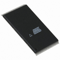
AT49F4096A-90TC Atmel, AT49F4096A-90TC Datasheet - Page 2

AT49F4096A-90TC
Manufacturer Part Number
AT49F4096A-90TC
Description
IC FLASH 4MBIT 90NS 48TSOP
Manufacturer
Atmel
Datasheet
1.AT49F4096A-90RC.pdf
(15 pages)
Specifications of AT49F4096A-90TC
Format - Memory
FLASH
Memory Type
FLASH
Memory Size
4M (512K x 8 or 256K x 16)
Speed
90ns
Interface
Parallel
Voltage - Supply
4.5 V ~ 5.5 V
Operating Temperature
0°C ~ 70°C
Package / Case
48-TSOP
Lead Free Status / RoHS Status
Contains lead / RoHS non-compliant
Available stocks
Company
Part Number
Manufacturer
Quantity
Price
Company:
Part Number:
AT49F4096A-90TC
Manufacturer:
ATM
Quantity:
3 586
Company:
Part Number:
AT49F4096A-90TC
Manufacturer:
ATM
Quantity:
3 586
Company:
Part Number:
AT49F4096A-90TC
Manufacturer:
TOSHIBA
Quantity:
4 130
Part Number:
AT49F4096A-90TC
Manufacturer:
ATMEL/爱特梅尔
Quantity:
20 000
block of data and then programming on a byte-by-byte or
word-by-word basis.
The device is erased by executing the erase command
sequence; the device internally controls the erase opera-
tion. The memory is divided into four blocks for erase oper-
ations. There are two 4K word parameter block sections,
the boot block, and the main memory array block. The typi-
cal number of program and erase cycles is in excess of
10,000 cycles.
The 8K word boot block section includes a reprogramming
lock out feature to provide data integrity. This feature is
enabled by a command sequence. Once the boot block
programming lockout feature is enabled, the data in the
2
AT49F4096A(T) SOIC (SOP)
I/O10
I/O11
GND
I/O0
I/O8
I/O1
I/O9
I/O2
I/O3
A17
NC
NC
CE
OE
A7
A6
A5
A4
A3
A2
A1
A0
1
2
3
4
5
6
7
8
9
10
11
12
13
14
15
16
17
18
19
20
21
22
AT49F004(T)/4096A(T)
44
43
42
41
40
39
38
37
36
35
34
33
32
31
30
29
28
27
26
25
24
23
RESET
WE
A8
A9
A10
A11
A12
A13
A14
A15
A16
BYTE
GND
I/O15/A-1
I/O7
I/O14
I/O6
I/O13
I/O5
I/O12
I/O4
VCC
RESET
A15
A14
A13
A12
A11
A10
A17
WE
NC
NC
NC
NC
NC
NC
A9
A8
A7
A6
A5
A4
A3
A2
A1
AT49F4096A(T) TSOP Top View
1
2
3
4
5
6
7
8
9
10
11
12
13
14
15
16
17
18
19
20
21
22
23
24
Type 1
boot block cannot be changed when input levels of 5.5
volts or less are used. The boot sector is designed to con-
tain user secure code.
For the AT49F4096A(T), the BYTE pin controls whether
the device data I/O pins operate in the byte or word config-
uration. If the BYTE pin is set at a logic “1” or left open, the
device is in word configuration, I/O0 - I/O15 are active and
controlled by CE and OE.
If the BYTE pin is set at logic “0”, the device is in byte con-
figuration, and only data I/O pins I/O0 - I/O7 are active and
controlled by CE and OE. The data I/O pins I/O8 - I/O14
are tri-stated and the I/O15 pin is used as an input for the
LSB (A-1) address function.
48
47
46
45
44
43
42
41
40
39
38
37
36
35
34
33
32
31
30
29
28
27
26
25
A16
BYTE
GND
I/O15 / A-1
I/O7
I/O14
I/O6
I/O13
I/O5
I/O12
I/O4
VCC
I/O11
I/O3
I/O10
I/O2
I/O9
I/O1
I/O8
I/O0
OE
GND
CE
A0
RDY/BUSY
RESET
A16
A15
A14
A13
A12
A11
A18
WE
NC
A9
A8
A7
A6
A5
A4
A3
A2
A1
AT49F004(T) TSOP Top View
1
2
3
4
5
6
7
8
9
10
11
12
13
14
15
16
17
18
19
20
Type 1
40
39
38
37
36
35
34
33
32
31
30
29
28
27
26
25
24
23
22
21
A17
GND
NC
NC
A10
I/O7
I/O6
I/O5
I/O4
VCC
VCC
NC
I/O3
I/O2
I/O1
I/O0
OE
GND
CE
A0


