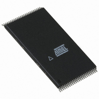
AT49BV322A-70TI Atmel, AT49BV322A-70TI Datasheet - Page 2

AT49BV322A-70TI
Manufacturer Part Number
AT49BV322A-70TI
Description
IC FLASH 32MBIT 70NS 48TSOP
Manufacturer
Atmel
Datasheet
1.AT49BV322A-70TI.pdf
(32 pages)
Specifications of AT49BV322A-70TI
Format - Memory
FLASH
Memory Type
FLASH
Memory Size
32M (4Mx8, 2Mx16)
Speed
70ns
Interface
Parallel
Voltage - Supply
2.65 V ~ 3.6 V
Operating Temperature
-40°C ~ 85°C
Package / Case
48-TSOP
Lead Free Status / RoHS Status
Contains lead / RoHS non-compliant
Available stocks
Company
Part Number
Manufacturer
Quantity
Price
Company:
Part Number:
AT49BV322A-70TI
Manufacturer:
ATMEL
Quantity:
5 530
Company:
Part Number:
AT49BV322A-70TI
Manufacturer:
ATMEL
Quantity:
4 125
Part Number:
AT49BV322A-70TI
Manufacturer:
ATMEL/爱特梅尔
Quantity:
20 000
The VPP pin provides data protection. When the V
input is below 0.4V, the program and erase
PP
functions are inhibited. When V
is at 0.9V or above, normal program and erase operations can
PP
be performed.
A six-byte command (Enter Single Pulse Program Mode) sequence to remove the requirement
of entering the three-byte program sequence is offered to further improve programming time.
After entering the six-byte code, only single pulses on the write control lines are required for writ-
ing into the device. This mode (Single Pulse Byte/Word Program) is exited by powering down
the device, or by pulsing the RESET pin low for a minimum of 500 ns and then bringing it back to
V
. Erase, Erase Suspend/Resume and Program Suspend/Resume commands will not work
CC
while in this mode; if entered they will result in data being programmed into the device. It is not
recommended that the six-byte code reside in the software of the final product but only exist in
external programming code.
The BYTE pin controls whether the device data I/O pins operate in the byte or word configura-
tion. If the BYTE pin is set at logic “1”, the device is in word configuration, I/O0 - I/O15 are active
and controlled by CE and OE.
If the BYTE pin is set at logic “0”, the device is in byte configuration, and only data I/O pins I/O0
- I/O7 are active and controlled by CE and OE. The data I/O pins I/O8 - I/O14 are tri-stated, and
the I/O15 pin is used as an input for the LSB (A-1) address function.
AT49BV322A(T)
2
3308J–FLASH–4/05


