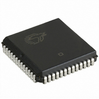
CY7C131-25JC Cypress Semiconductor Corp, CY7C131-25JC Datasheet - Page 3

CY7C131-25JC
Manufacturer Part Number
CY7C131-25JC
Description
IC SRAM 8KBIT 25NS 52PLCC
Manufacturer
Cypress Semiconductor Corp
Specifications of CY7C131-25JC
Format - Memory
RAM
Memory Type
SRAM - Dual Port, Asynchronous
Memory Size
8K (1K x 8)
Speed
25ns
Interface
Parallel
Voltage - Supply
4.5 V ~ 5.5 V
Operating Temperature
0°C ~ 70°C
Package / Case
52-PLCC
Density
8Kb
Access Time (max)
25ns
Sync/async
Asynchronous
Architecture
Not Required
Clock Freq (max)
Not RequiredMHz
Operating Supply Voltage (typ)
5V
Address Bus
10b
Package Type
PLCC
Operating Temp Range
0C to 70C
Number Of Ports
2
Supply Current
170mA
Operating Supply Voltage (min)
4.5V
Operating Supply Voltage (max)
5.5V
Operating Temperature Classification
Commercial
Mounting
Surface Mount
Pin Count
52
Word Size
8b
Number Of Words
1K
Lead Free Status / RoHS Status
Contains lead / RoHS non-compliant
Other names
428-1193
Available stocks
Company
Part Number
Manufacturer
Quantity
Price
Company:
Part Number:
CY7C131-25JC
Manufacturer:
CYP
Quantity:
5 510
Company:
Part Number:
CY7C131-25JC
Manufacturer:
Cypress Semiconductor Corp
Quantity:
10 000
Part Number:
CY7C131-25JC
Manufacturer:
CYPRESS/赛普拉斯
Quantity:
20 000
Electrical Characteristics
Capacitance
]
Parameter
V
V
V
V
I
I
I
I
I
I
I
I
Notes:
C
C
10. At f=f
IX
OZ
OS
CC
SB1
SB2
SB3
SB4
6.
7.
8.
9.
OH
OL
IH
IL
IN
OUT
See the last page of this specification for Group A subgroup testing information.
BUSY and INT pins only.
Duration of the short circuit should not exceed 30 seconds.
This parameter is guaranteed but not tested.
Parameter
MAX
, address and data inputs are cycling at the maximum frequency of read cycle of 1/t
Output HIGH
Voltage
Output LOW
Voltage
Input HIGH Voltage
Input LOW Voltage
Input Leakage
Current
Output Leakage
Current
Output Short
Circuit Current
V
Supply Current
Standby Current
Both Ports,
TTL Inputs
Standby Current
One Port,
TTL Inputs
Standby Current
Both Ports,
CMOS Inputs
Standby Current
One Port,
CMOS Inputs
CC
[9]
Description
Operating
Input Capacitance
Output Capacitance
[8, 9]
Description
Over the Operating Range
V
I
I
GND < V
GND < V
Output Disabled
V
V
CE = V
Outputs Open,
f = f
CE
V
CE
Active Port Out-
puts Open,
f = f
Both Ports CE
and CE
0.2V,
V
or V
One Port CE
CE
V
or V
Active Port Outputs
Open,
f = f
OL
OL
CC
CC
OUT
IH
IN
IN
L
L
R
, f = f
MAX
= 4.0 mA
= 16.0 mA
MAX
MAX
> V
> V
IN
IN
Test Conditions
= Min., I
= Max.,
and CE
or CE
> V
= GND
< 0.2V, f = 0
< 0.2V,
[10]
IL
CC
CC
R
[10]
[10]
MAX
CC
,
I
O
> V
< V
R
– 0.2V
– 0.2V
< V
– 0.2V,
R
[10]
OH
> V
CC
L
CC
[7]
>
L
CC
or
= –4.0 mA
IH
–
,
,
Com’l
Mil
Com’l
Mil
Com’l
Mil
Com’l
Mil
Com’l
Mil
T
V
A
CC
= 25 C, f = 1 MHz,
= 5.0V
[6]
7C131-15
Min.
3
2.4
2.2
7C141-15
–5
–5
Test Conditions
Max.
–350
RC
190
135
125
0.4
0.5
0.8
+5
+5
75
15
[3,4]
and using AC Test Waveforms input levels of GND to 3V.
7C131-25,30
7C141-25,30
Min.
7C130-30
2.4
2.2
–5
–5
7C140-30
Max. Min. Max.
–350
170
115
105
0.4
0.5
0.8
+5
+5
65
15
[3]
7C130-35
7C131-35
7C140-35
7C141-35
2.4
2.2
CY7C130/CY7C131
CY7C140/CY7C141
–5
–5
–350
120
170
105
115
0.4
0.5
0.8
+5
+5
45
65
90
15
15
85
Max.
15
10
7C130-45,55
7C131-45,55
7C140-45,55
7C141-45,55
Min.
2.4
2.2
–5
–5
Max. Unit
–350
120
0.4
0.5
0.8
+5
+5
90
35
45
75
90
15
15
70
85
Unit
pF
pF
mA
mA
mA
mA
mA
mA
V
V
V
V
A
A


