CY62128BLL-70SXC Cypress Semiconductor Corp, CY62128BLL-70SXC Datasheet - Page 5
CY62128BLL-70SXC
Manufacturer Part Number
CY62128BLL-70SXC
Description
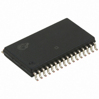
IC SRAM 1MBIT 70NS 32SOIC
Manufacturer
Cypress Semiconductor Corp
Specifications of CY62128BLL-70SXC
Format - Memory
RAM
Memory Type
SRAM
Memory Size
1M (128K x 8)
Speed
70ns
Interface
Parallel
Voltage - Supply
4.5 V ~ 5.5 V
Operating Temperature
0°C ~ 70°C
Package / Case
32-SOIC (11.30mm Width)
Lead Free Status / RoHS Status
Lead free / RoHS Compliant
Other names
428-1746-5
CY62128BLL-70SXC
CY62128BLL-70SXC
Available stocks
Company
Part Number
Manufacturer
Quantity
Price

Company:
Part Number:
CY62128BLL-70SXCT
Manufacturer:
FSC
Quantity:
15 400


Document #: 38-05300 Rev. *C
Switching Characteristics
Switching Waveforms
Read Cycle No.1
Notes:
10. The internal write time of the memory is defined by the overlap of CE
11. No input may exceed V
12. Device is continuously selected. OE, CE
13. WE is HIGH for read cycle.
READ CYCLE
t
t
t
t
t
t
t
t
t
t
t
WRITE CYCLE
t
t
t
t
t
t
t
t
t
t
7.
8.
9.
RC
AA
OHA
ACE
DOE
LZOE
HZOE
LZCE
HZCE
PU
PD
WC
SCE
AW
HA
SA
PWE
SD
HD
LZWE
HZWE
Parameter
DATA OUT
ADDRESS
Test conditions assume signal transition time of 5 ns or less, timing reference levels of 1.5V, input pulse levels of 0 to 3.0V, and output loading of the specified
I
t
At any given temperature and voltage condition, t
and the transition of any of these signals can terminate the write. The input data set-up and hold timing should be referenced to the leading edge of the signal that terminates
the write.
OL
HZOE
/I
OH
, t
HZCE
and 100-pF load capacitance.
, and t
[10]
Read Cycle Time
Address to Data Valid
Data Hold from Address Change
CE
OE LOW to Data Valid
OE LOW to Low Z
OE HIGH to High Z
CE
CE
CE
CE
Write Cycle Time
CE
Address Set-up to Write End
Address Hold from Write End
Address Set-up to Write Start
WE Pulse Width
Data Set-up to Write End
Data Hold from Write End
WE HIGH to Low Z
WE LOW to High Z
HZWE
[12, 13]
1
1
1
1
1
1
are specified with a load capacitance of 5 pF as in (b) of AC Test Loads. Transition is measured ±500 mV from steady-state voltage.
LOW to Data Valid, CE
LOW to Low Z, CE
HIGH to High Z, CE
LOW to Power-up, CE
HIGH to Power-down, CE
LOW to Write End, CE
CC
+ 0.5V.
PREVIOUS DATA VALID
[7]
1
Over the Operating Range
= V
[9]
[8, 9]
[7, 9]
IL
, CE
t
Description
2
OHA
2
HZCE
HIGH to Low Z
2
LOW to High Z
= V
2
2
2
HIGH to Power-up
HIGH to Write End
is less than t
IH
HIGH to Data Valid
.
2
LOW to Power-down
t
AA
LZCE
1
[9]
, t
[8, 9]
LOW, CE
HZOE
is less than t
t
2
RC
HIGH, and WE LOW. CE
LZOE
, and t
HZWE
Min.
55
55
45
45
45
25
62128B-55
5
0
0
0
5
0
0
5
is less than t
1
and WE must be LOW and CE
Max.
55
55
20
20
20
55
20
LZWE
DATA VALID
for any given device.
Min.
70
70
60
60
50
30
62128B-70
5
0
5
0
0
0
0
5
2
CY62128B
HIGH to initiate a write,
Max.
70
70
35
25
25
70
25
MoBL
Page 5 of 11
Unit
ns
ns
ns
ns
ns
ns
ns
ns
ns
ns
ns
ns
ns
ns
ns
ns
ns
ns
ns
ns
ns
®
[+] Feedback
Related parts for CY62128BLL-70SXC
Image
Part Number
Description
Manufacturer
Datasheet
Request
R

Part Number:
Description:
IC SRAM 1MBIT 70NS 32SOIC
Manufacturer:
Cypress Semiconductor Corp
Datasheet:

Part Number:
Description:
IC SRAM 1MBIT 70NS 32TSOP
Manufacturer:
Cypress Semiconductor Corp
Datasheet:
Part Number:
Description:
IC SRAM 1MBIT 70NS 32TSOP
Manufacturer:
Cypress Semiconductor Corp
Datasheet:

Part Number:
Description:
IC SRAM 1MBIT 70NS 32TSOP
Manufacturer:
Cypress Semiconductor Corp
Datasheet:
Part Number:
Description:
IC SRAM 1MBIT 70NS 32TSOP
Manufacturer:
Cypress Semiconductor Corp
Datasheet:
Part Number:
Description:
Manufacturer:
Cypress Semiconductor Corp
Datasheet:
Part Number:
Description:
Manufacturer:
Cypress Semiconductor Corp
Datasheet:
Part Number:
Description:
Manufacturer:
Cypress Semiconductor Corp
Datasheet:

Part Number:
Description:
Manufacturer:
Cypress Semiconductor Corp
Datasheet:
Part Number:
Description:
Manufacturer:
Cypress Semiconductor Corp
Datasheet:
Part Number:
Description:
Manufacturer:
Cypress Semiconductor Corp
Datasheet:
Part Number:
Description:
Manufacturer:
Cypress Semiconductor Corp
Datasheet:
Part Number:
Description:
Manufacturer:
Cypress Semiconductor Corp
Datasheet:
Part Number:
Description:
Manufacturer:
Cypress Semiconductor Corp
Datasheet:
Part Number:
Description:
Manufacturer:
Cypress Semiconductor Corp
Datasheet: